Kapitoly z nanoelektroniky Nanoelectronic Chapters (koordinuje prof. E. Hulicius, FZÚ AV ČR, v.v.i.)
|
|
|
- Richard Josef Liška
- před 8 lety
- Počet zobrazení:
Transkript
1 Přednášky pro TU v Liberci Studijní program: Nanotechnologie Studijní obor: Nanomateriály (organizuje prof. J. Šedlbauer, FPP TU v Liberci) Kapitoly z nanoelektroniky Nanoelectronic Chapters (koordinuje prof. E. Hulicius, FZÚ AV ČR, v.v.i.) Čtyřhodinové bloky. Letní semestr 2016/2017 (to jest od února 2017 do června 2017). Zkouška (hlavně podle kvality a prezentace semestrální práce a případně podle znalostí převážně z oboru přiléhajícího k práci).
2 Semestrální práce: Přednášející vypíší témata ze svého oboru, ze kterých si studenti vyberou a zpracují je pod dohledem dotyčného přednašeče formou seminární práce (5-15 str.) a přednesou svým kolegům během jedné či dvou posledních čtyřhodinovek a za to obdrží známku. Mělo by jít o aktuální "state of art" daného tématu (které by mělo jistým způsobem doplňovat příslušnou přednášku), zpracovaného tak, aby srozumitelně poskytl svým kolegům novou a zajímavou informaci. Témata prací jsou na konci sylabů této přednášky. Téma je možné domluvit si individuálně s přednášejícím podle zájmu. Zkouška předmětu Kapitoly z nanoelektroniky spočívá hlavně ve vypracování a přednesení a obhájení seminární práce a případně ještě v zodpovězení otázek z bloku, ze kterého je tato seminární práce (pochybnosti učitele o známce, student ji chce lepší,...).
3 Příklady témat semestrálních prací z Kapitol o nanostrukturách 2016 Blok E. Huliciuse (hulicius@fzu.cz) (a badatelů z Fyzikálního ústavu AV ČR, Praha 6, Cukrovarnická 10; je: jmeno.přímení@fzu.cz Martin Nikl a Vítěslav Jarý: 1) Kvantové tečky a nanokrystaly - stavební kameny pro nanopráškové a nanokompozitní scintilátory. Jiří J. Mareš a Pavel Hubík 2) Transport v nitridových strukturách. Eduard Hulicius: 3) Aplikace polovodičových Kvantových teček nejen v LD. 4) Jaké jsou na českém trhu LEDky barva, výkon, cena, rizika (modrá složka světla). 5) Jaké jsou na českém trhu LD (laserové diody) barva, výkon, cena, rizika (výkon, hustota výkonu). Alice Hospodková: 6) Polovodičové nitridové nanostruktury pro LED. 7) Polovodičové nitridové nanostruktury pro HEMT. 8) Polovodičové nitridové nanostruktury pro scintilátory. Pavel Rossner prossner@biomed.cas.cz : 9) Antibakteriální působeni nanočástic kladné a záporné efekty. 10) Ekotoxicita vliv na životní prostředí. Antonín Fejfar + Martin Ledinský: 11) Nanostrukturované sluneční články. 12) Perovskitove vrstvy pro fotovoltaiku. Alexander Kromka: Maximálně tři témata z: 13) Růst diamantových tenkých vrstev (chemická depozice z par, mikrovlnná plazma, alternativní CVD techniky). 14) Tvorba funkčních opto-elektrických diamantových prvků (plazmatické iontové leptání, selektivní růst, nanodrátky, nanosloukpy, porézní vrstvy). 15) Diamantové vrstvy jako multifunkční substrátu pro tkáňové inženýrství a regenerativní medicínu (povrchová terminace, mikro vs. nano morfologie, optická průhlednost, biokompatibilita). 16) Diamantové vrstvy v senzorice (povrchová a objemová vodivost, chemické a biologické senzory, FETs a impedanční senzorové prvky, dozimetrie). 17) Diamant ve spinotronice (dopování a tvorba vakancí, fotoluminiscence, opticky aktivní centra). 18) Diamantové vrstvy pro MEMS/NEMS struktury. 19) Nanodiamanty v bio-inženýrství (tvorba diamantových nanočástic a jejich aplikace pro bio-zobrazování, cílený transport léků, kompozitní materiály, ).
4 Příklady témat semestrálních prací z Kapitol o nanostruktůrách 2016 pokračování: Blok E. Huliciuse (hulicius@fzu.cz) (a badatelů z Fyzikálního ústavu AV ČR, Praha 6, Cukrovarnická 10; je: jmeno.přímení@fzu.cz Ivan Gregora: 20) Ramanova Spektroskopie pro nanomateriály. Jiří Oswald: 21) Ramanova a luminiscenční mikrospektroskopie nitridových nanostruktur. Bohuslav Rezek: Maximálně tři témata z: Nabídka témat semestrálních (souhrn na základě rešerše literatury, naše i cizí publikace, s možností pokračovat jako diplomka) 22) Přínosy a problémy využití nanočástic ve fotovoltaických prvcích. 23) Využití nanočástic pro elektronické senzory molekul. 24) Fluorescenční sledování molekul pomocí anorganických nanočástic. 25) Vliv nanostruktury a elektrického náboje na interakci vody s povrchy. 26) Vliv podložky na elektrostat. náboj nanočástic z různých materiálů (diam, Au, Si, SiO2). 27) Vliv podložky na elektronické vlastnosti (nabíjení) moderních 2D materiálů (graphene, GO/rGO, MoS, black phosphorus). 28) Jak měřit elektrickou vodivost nanočástic. 29) Jak měřit elektrický potenciál nanočástic s vysokým časovým rozlišením. 30) Metody pro řízené samouspořádávání nanočástic na povrchu. 31) Srovnání komerčně dostupných nanodiamantů a jejich vlastností. Jiří Červenka: 32) Aplikace grafenu v nanoelektronice příprava nových grafenových tranzistorů. 33) Grafenové sensory detekce plynů. 34) Grafenové sensory detekce biomolekul A kdo chce, může oslovit libovolného zajímavého přednašeče a domluvit se s ním. Kontaktní osoba poskytne podklady, konzultace a přečte elaborát. Každé téma lze případně rozvést do diplomové, v některých případech i do disertační (doktorské) práce.
5 Chapters on nanoelectronics E. Hulicius, FZÚ AV ČR, v.v.i.
6 Technology of nanostructure preparation, nano-heterostructures A III B V (quantum dots and wells) preparation, properties, applications E. Hulicius, FZÚ AV ČR, v. v. i. (hulicius@fzu.cz) 0. What does it means nano. Are current definitions correct? 1. Epitaxial growth of layers and structures - Principles, phases and types of growth. Sorts of epitaxy epitaxy from solid, liquid and gas phases. Epitaxial growth from the material point of view. 2. Epitaxial techniques for semiconductor nanostructures preparation The fundamental methods are Epiataxy from molecular beams (Molecular Beam Epitaxy - MBE) and gas epitaxy from organometalic compounds (MetalOrganic Vapour Phase Epitaxy - MOVPE). Detail descriptions of both techniques, comparison, differences, limits, fields of application, parameters of chosen structures. Growth of QW, QWr, QD and quantum cascade structures. Short history of both technologies development.
7 Technology of nanostructure preparation, nano-heterostructures A III B V (quantum dots and wells) preparation, properties, applications 3. Characterisation "in situ" techniques - Description of the electron, optical, structural methods. Implementation of these methods during epitaxial growth. Their limits due to using during growth in situ. Possible recommended literature (available at the lecturer): V.A. Schuskin, N.N. Ledentsov, D. Bimberg, Epitaxy of Nanostructures, Springer- Verlag, Berlin Heidelberg New York 2004, ISBN M.A. Herman, W. Richter, H. Sitter, Epitaxy, Springer-Verlag, Berlin Heidelberg New York 2004, ISBN Guozhong Gao, Nanostructures and Nanomaterials, Imperial College Press, London 2004, ISBN V.M. Ustinov, A.E. Zhukov, A.Y. Egorov, N.A. Maleev, Quantum dot lasers, Oxford University Press, 2003, ISBN
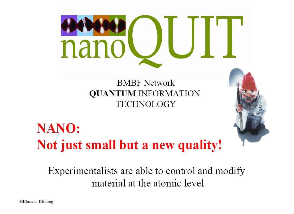
8 In general: NANO is not only because it is small! Quantum effect starts to be fundamental.
9
10
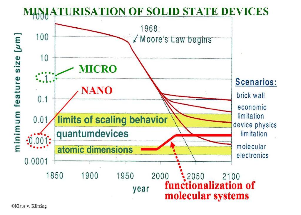
11 Well known Moor law (about exponential decreasing of size of electronic devices and subsequent increasing of memory and speed), its history and potential future scenarios. Context with NANO. Quantum effects.
12
13
14
15

16
17
18
19 Optical lithography, which has been the predominant patterning technique since the advent of the semiconductor age, is capable of producing sub-100-nm patterns with the use of very short optical wavelengths. Several optical lithography techniques require the use of liquid immersion and a host of resolution enhancement technologies like phase-shift masks (PSM) and optical proximity correction (OPC). Multiple patterning is a method of increasing the resolution by printing features in between pre-printed features on the same layer by etching or creating sidewall spacers, and has been used in commercial production of microprocessors since the 32 nm process node e.g. by directed self-assembly (DSA). Extreme ultraviolet lithography (EUVL) uses ultrashort wavelengths (13.5 nm) and as of 2015, is the most popularly considered Next-generation lithography (NGL) technique for mass-fabrication. [1]
20 Electron beam lithography or Electron-Beam Direct-Write Lithography (EBDW) scans a focused beam of electrons on a surface covered with an electron-sensitive film or resist (e.g. PMMA or HSQ) to draw custom shapes. By changing the solubility of the resist and subsequent selective removal of material by immersion in a solvent, sub-10 nm resolutions have been achieved. This form of direct-write, mask-less lithography has high resolution and low throughput, limiting single-column e-beams to photomask fabrication, low-volume production of semiconductor devices, and research&development. Multiple-electron beam approaches have as a goal an increase of throughput for semiconductor mass-production.
21 Nanoimprint lithography (NIL), and its variants, such as Step-and- Flash Imprint Lithography, LISA and LADI are promising nanopattern replication technologies where patterns are created by mechanical deformation of imprint resist, typically amonomer or polymer formulation that is cured by heat or UV light during imprinting. This technique can be combined with contact printing and cold welding.
22 Scanning probe lithography (SPL) is a tool for patterning at the nanometer-scale down to individual atoms using scanning probes. Dippen nanolithography is an additive, diffusive method, thermochemical nanolithography triggers chemical reactions, thermal scanning probe lithography creates 3D surfaces from polymers, and local oxidation nanolithography employs a local oxidation reaction for patterning purposes.
23 Other techniques Molecular self-assembly (as bottom-up approach) of dense lines less than 20 nm wide in large prepatterned trenches has been demonstrated. [2] Aligned arrays of plasmonic [3] and magnetic wires and nanoparticles are deposited on these templates via oblique evaporation. The templates are easily produced over large areas with periods down to 25 nm. Stencil lithography is a resist-less and parallel method of fabricating nanometer scale patterns using nanometer-size apertures as shadow-masks. X-ray lithography can be extended to a resolution of 15 nm by using the X-ray wavelengths of 1 nm as illumination. This is implemented by the proximity printing approach. The method is simple because it requires no lenses. Laser printing of single nanoparticles In this method, the optical forces induced via scattering and absorption of photons on nanoparticles are used to direct single nanoparticles to specific locations on substrates and attach them via van-der Waals forces. This technique has been demonstrated on metallic nanoparticles, Magnetolithography (ML) based on applying a magnetic field on the substrate using paramagnetic metal masks call "magnetic mask". Magnetic mask which is analog to photomask define the spatial distribution and shape of the applied magnetic field. Nanosphere lithography uses self-assembled monolayers of spheres (typically made of Polystyrene) as evaporation masks. This method has been used to fabricate arrays of gold nanodots. Proton beam writing uses a focused beam of high energy (MeV) protons to pattern resist material at nanodimensions. Charged-particle lithography, such as ion- or electron-projection lithographies (PREVAIL, SCALPEL, LEEPL), are also capable of high-resolution patterning. Ion beam lithography uses a focused or broad beam of energetic lightweight ions (like He + ) Neutral particle lithography uses a broad beam of energetic neutral particle for pattern transfer on a surface.
24
25 Paradigma of the quantum dots Moving from atomic electron levels over electron (hole) energy band structures to again discrete electron (hole) energy levels. Fundamental role of NANO. Quantum effects.
26 Atom - Solid state - Quantum dot
27
28 Procedures: Bottom-up a Top-down and also something between Examples of preparation or creations of the nanostructures Top-down cutting Bottom-up building something between self made self-assembled

29
30 Nanostructure preparation can be very simple...
31
32 or very complicated, difficult and expensive:
33

34

35

36 Elektroluminiscenční displeje QLED vytvořené pomocí kvantových teček mají oproti dosavadním displejům hodně výhod. Tenké displeje s přesným a kontrastním vykreslováním tvarů a barev dobývají svět. Vývoj se nezastaví u dnešních displejů typu LCD nebo LED, popř. U displejů na bázi organických polymerů, tzv. OLED. Několik firem teď přichází s pokročilou technologií elektroluminiscence, která je založena na tzv. kvantových tečkách. Jedná se o displeje QLED. Kvantové tečky jsou ostře lokalizované krystalické oblasti polovodiče o nanometrových rozměrech. Kvantové tečky jsou schopny vázat jednotlivé elektrony a pracovat s nimi, případně jsou schopny produkovat fotony,které lze použít v dalším kroku. Elektroluminiscence označuje jev, při kterém lze v určitém materiálu řídit vyzařování světla pomocí elektrického proudu nebo elektrického pole.

37 Čtyři rozdílné barvy odpovídají čtyřem druhům kvantových teček. Foto: Padova University Raffaella Signorini

38
39


40
41


42 Aplikace Nanostruktur
43 Future R&D Directions of NMP Programme for the Period Materials Science and Engineering 3.1 Present State-of-the-art 3.2 Cross-cutting Research Directions in Materials Materials by Design: Synthesis, Characterization, Processing & Modelling Understanding Surfaces and Interfacial Phenomena Design and Manufacturing of Multifuctional Materials Design and Manufacturing of Structural Materials Integration of Multiple-Scale Phenomena (Molecular, Nano and Micro) in Materials Design and Production Development of Computational Tools for Predicting Functional and Structural Properties of Materials Metrology, Instrumentation: New Analytical Tools for Measurement of Materials Functional and Structural Properties 3.3 Materials Applications for Selective Industrial Sectors Materials for Information Technologies Biomaterials, Biomimetcs and Biomedical Engineering Materials for Energy Applications Surface Engineering and Coatings Catalysis and Chemicals Technologies Polymers, Composites and Hybrid Materials Renewable Materials, Ecomaterials Disassembly Recovery and Recycle of Materials 3.4 Recommendations and Priority Research Directions
44 Future R&D Directions of NMP Programme for the Period Industrial Production Systems 4.1 Present State-of-the-art 4.2 Cross-Cutting Research Directions in Manufacturing New Business Models Adaptive Manufacturing Networking in Manufacturing Digital Knowledge-based Engineering Emerging Technologies ICT for Manufacturing 4.3 Exploitation of the Convergence of Technologies Next-generation HVA Products Education and training in Learning Factories Disruptive Factory: Bio-nano convergence Disruptive Factory: Bio-cogno-ICT convergence 4.4 Cross-cutting Research Directions in Production Systems Batch and Continuous Production Systems Scale-up, Scale-down Developments and Process Intensification Enabling Technologies (e.g., On-line Monitoring, On-line Sensors, Process Optimization and Control, Supply Chain Management) Digital Production (integration of product design and production systems) New Products/Services and New Production Paradigms Alternative, Renewable and Novel Feedstocks and Processes for Chemicals and Materials Production 4.5 Recommendations and Priority Research Directions
45 EPITAXIAL TECHNOLOGY in general Eduard Hulicius Laboratoř MOVPE, Oddělení polovodičů, Fyzikální ústav AV ČR Praha 6, Cukrovarnická Web FZÚ AV ČR, v.v.i. Brána pro veřejnost
46 Epitaxial technology Name epitaxe origins from Greek epi-taxis which means arranged on" was introduced by L. Royer at It is monocrystalic growth on (usually) monocrystalic substrate (wafer). Growth is not (usually) epitaxial when lattice constant difference is bigger than 15%. Explanation of importance and principles and comparison with other monocrystal preparation methods Why so monstrous, expensive, danger and demanding technology equipments Preparation and properties of the bulk crystals. Epitaxial growth advantages, new possibilities, limits. Homo- and heteroepitaxy. Equation of minimum of energy. Principle of the epitaxial growth. Atoms or molecules of the compound, which we would like to deposit on suitable substrate, are transported to its surface, which have to be atomically clean cleaned from oxides and sorbants - and atomically smooth (only with atomic steps due to disorientation of the monocrystalic substrate). On the surface the atoms will be physysorbed, and after that chemisorbed to the crystal structure. By this way atomic layers and all structure are grown.
47 Preparation and properties of the bulk crystals:

48 Preparation and properties of the bulk crystals:


49 Growth of monocrystals by the Czochralsky method


50 Polovodičové (mono)krystaly i jiné:


51 Polovodičové (mono)krystaly konference Berlin 2011
52 Růst monokrystalů metodou horizontální Bridgman
53 Růst monokrystalů metodou horizontální Bridgman
54 Růst monokrystalů metodou horizontální Bridgman

55 Růst monokrystalů metodou horizontální Bridgman
56 Bulk monocrystals, have impresive parametres - (atomic periodicity of monocrystal lattice more than one meter!), but they are not crystalographicly perfect nad for majority of electronic, namely optoelectronic, applications are not suitable. The reason is high temperature during their creation from melted material. We have to prepare materials and structures using epitaxial technologies which work at lower temperatures.
57 Epitaxy technologies Name epitaxe origins from Greek epi-taxis which means arranged on" was introduced by L. Royer at It is monocrystalic growth on (usually) monocrystalic substrate (wafer). Growth is not (usually) epitaxial when lattice constant difference is bigger than 15%. Explanation of importance and principles and comparison with other monocrystal preparation methods Why so monstrous, expensive, danger and demanding technology equipments Preparation and properties of the bulk crystals. Epitaxial growth advantages, new possibilities, limits. Homo- and heteroepitaxy. Equation of minimum of energy. Principle of the epitaxial growth. Atoms or molecules of the compound, which we would like to deposit on suitable substrate, are transported to its surface, which have to be atomically clean cleaned from oxides and sorbants - and atomically smooth (only with atomic steps due to disorientation of the monocrystalic substrate). On the surface the atoms will be physysorbed, and after that chemisorbed to the crystal structure. By this way atomic layers and all structure are grown.
58 Epitaxy technologies Epitaxial growth of monocrystalic layers (on the bulk monocrystal wafers = substrates) is realised at lower temperature than growth of monocrystals from melted material, which is substantial for: Influence of the enthropy (native defects), lower solutibility of the unintentional impurities into the prepared layers. Nevertheless this lower temperature (usually around 500 C) is high enough for creation of atomically clean and flat surface and enable atoms jump over the energy barriers for physisorption and chemisorption.
59 Chemický stav daného systému dobře popisuje chemický potenciál μ. Pro danou fázi je definován jako vzrůst volné Gibbsovy energie δg když se přidá jeden mol látky při konstantní teplotě a tlaku μ = δg/δn/ T,p Vyjádříme-li molarní Gibbsovu energii ΔG pomocí enthalpie ΔH a entropie ΔS μ = ΔG = ΔH - TΔS což lze po dosazení používat k výpočtům.
60
61
 Ostrůvky na substrátu Volmerův-Weberův e) Sloupkový")
62 Druhy epitaxních růstů a) Vrstva po vrstvě Frankův-van der Merweův růst b) Vrstva po vrstvě - spojitě c) Ostrůvky na smáčecí vrstvě - Stranského-Krastanowův d) Ostrůvky na substrátu Volmerův-Weberův e) Sloupkový růst
63 Typy epitaxních růstů a vysvětlení různých používaných zkratek: Epitaxe z pevné fáze Epitaxe z kapalné fáze Epitaxe z plynné fáze SPE (Solid Phase Epitaxy) LPE (Liquid Phase Epitaxy) LPEE (Liquid Phase Electroepitaxy) VPE (Vapour (Vapor) Phase Epitaxy) CVD (Chemical Vapour Deposition) PVD (Physical Vapour Deposition)
64 Hlavní typy VPE epitaxních růstů Molekulární epitaxe - MBE (Molecular beam epitaxy) SSMBE = SolidSource MBE, CBE = ChemicalBeamEpitaxy, GSMBE = GasSource MBE (HydrideSource MOMBE, MetalOrganic MBE), UHV ALE = UltraHighVacuum AtomicLayerEpitaxy Plynná epitaxe z organokovových sloučenin - MOVPE (MetalOrganic Vapour Phase Epitaxy) MOCVD (MetalOrganic Chemical Vapour Deposition) Photo-MOVPE (Netermální, světlem. aktivov.) Plasma-MOVPE (Netermální, plasm. aktivov.)
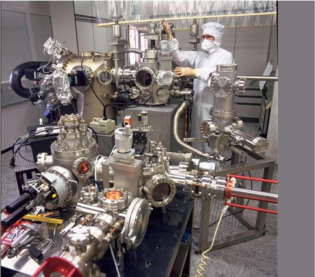
65 Solid State Epitaxy - SPE The old method with new applications. Metastable amorphous phase of solid state material, which is in touch with monocrystal, gradually assume crystalline form starting from the junction, copy monocrystal lattice, but with much lower point defect concentration. Growth speed usually nm per second is controlled by activation energy SPE E a : v = v 0 exp (-E a /kt) Applications: Preparation of thick semiconductor epitaxial layers with high doping. Low temperature epitaxy (Ga(Mn)As spinotronics?). Growth of the buffer layers for improving of properties of heterostructures decreasing dislocation densities - Nitrides! Silicide layers for electric contacts and Schottky barriers for Si devices.
66 Steps of the Solid State Epitay:
67
68 Liquid Phase Epitaxy - LPE The most important epitaxial method during seventies and eighties of the last century. Still using in the industry (cheap LEDs and when tens of micrones are necessary). Important for thermodynamical equilibrium grown structures. Princip of the LPE: Saturated solution of suitable materials (e.g. As in Ga) is cooling (or the liquid part is evaporated this is not realistic for Ga (it has low vapour pessure)) and thus starts to be oversaturated, thus As is going out from solution and created GaAs on the reasonable bulk or epitaxial substrate.
69
70 Vapour phase Epitaxy - VPE Todayand at least next ten years it will be the most important semiconductor preparation technology not only for industry but also for research. In principle it is possible to describe it as physical (PVD - Physical Vapour Deposition) and chemical (CVD - Chemical Vapour Deposition), according the transport of material from the source to the substrate. At first PVD it is evaporation of atoms or molecules (using heat, sputtering, ablation, discharge, etc.) without their chemical changes. At second CVD it is transport of volatile chemical compounds (precursors) using some transport gases (H2, N2) to the heated substrate near of its surface their are decomposed. Epitaxial growth on atomically clean and flat surface of usually monocrystalical substrate (wafer) is then similar. Also parameters of prepared layers are similar. In both cases we need extreme semiconductor cleanness vacuum (10-10 torr) or transport gas H 2 či N 2 (at the level of fractions of ppb).
71 Examples: Halide epitaxy Metals or elementary semiconductors - (WF 6 W +..., SiCl 4 Si +...) Compound semiconductors - (GaCl + AsH 3 GaAs +...) Granits of rare earths - (YCl 3 + FeCl 2 + O 2 Y 3 Fe 5 O ) Oxide epitaxy Compound semiconductors - (GaO 2 + PH 4 GaP +...) Hydride epitaxy Elementary semiconductors, very important silicon - (SiH 4 Si +...) Izolating layers: oxides, nitrides - (SiH 4 + H 2 O SiO ; SiH 4 + NH 3 Si 3 N ) Organometalic epitaxy Compound semiconductors - (Ga(CH 3 ) 3 + AsH 3 GaAs +...) Metals - (Al(C 4 H 9 ) 3 Al +...) High-temperature supraconductors YBaCuO
72 Main types of VPE growths Molecular epitaxy - MBE (Molecular beam epitaxy) SSMBE = SolidSource MBE, CBE = ChemicalBeamEpitaxy, GSMBE = GasSource MBE (HydrideSource MOMBE, MetalOrganic MBE), UHV ALE = UltraHighVacuum AtomicLayerEpitaxy Vapour epitaxy from organometalic compounds - MOVPE (MetalOrganic Vapour Phase Epitaxy) MOCVD (MetalOrganic Chemical Vapour Deposition) Photo-MOVPE (Nonthermal, light activated) Plasma-MOVPE (Nonthermal, plasma activated)
73 The most important for nanotechnology are MBE and MOVPE Molecular beam epitaxy - MBE We can sort it according the sources o the molecular beams: Solid Source MBE, Gas Source MBE (or Chemical Beam Epitaxy) Hydride Source MBE, MetalOrganic MBE, Schema and photos of different equipments produced by some producers:


74 Zdroj:

75
76


77
78 Molecular beam epitaxy Principle of method: Substrate(s) is heated in the high vacuum (10 -(9-10) torr) up to so high temperature when native oxides and surface impurities are desorbed and surface of the substrate is atomically clean. Then preheated Knudsen (effusion) cell will be open and atoms or molecules fly several tens centimetres without collisions through growth chamber on the substrate (they are also evaporated at the vicinity of substrate). Atoms of future epitaxial layer sit on the surface (physisorption) moving to the proper crystallographic sites where they are bounded (chemisorption). By this way the epitaxil layer is created. Substrate is monocrystallic semiconductor wafer with diameter from 2 to 8 inches, which is μm thick. Questions?
79 Expected questions: Why this substrate size? How input and také out substrate? What is maximal size of substrate(s)? Substrate(s) is heated in the high vacuum (10-(9-10) torr) up to so high temperature when native oxides and surface impurities are desorbed and surface of the substrate is atomically clean. Then preheated Knudsen (effusion) cell will be open and atoms or molecules fly several tens centimetres without collisions through growth chamber on the substrate (they are also evaporated at the vicinity of substrate). Atoms of future epitaxial layer sit on the surface (physisorption) moving to the proper crystallographic sites where they are bounded (chemisorption). By this way the epitaxil layer is created. Substrate is monocrystallic semiconductor wafer with diameter from 2 to 8 inches, which is μm thick.
80 Expected questions: Why this substrate size? How input and také out substrate? What is maximal size of substrate(s)? Why substrate rotates? Substrate(s) is heated in the high vacuum (10-(9-10) torr) up to so high temperature when native oxides and surface impurities are desorbed and surface of the substrate is atomically clean. Then preheated Knudsen (effusion) cell will be open and atoms or molecules fly several tens centimetres without collisions through growth chamber on the substrate (they are also evaporated at the vicinity of substrate). Atoms of future epitaxial layer sit on the surface (physisorption) moving to the proper crystallographic sites where they are bounded (chemisorption). By this way the epitaxil layer is created. Substrate is monocrystallic semiconductor wafer with diameter from 2 to 8 inches, which is μm thick.
81 Expected questions: Why this substrate size? How input and také out substrate? What is maximal size of substrate(s)? Why substrate rotates? Why so high vacuum is necessary? Substrate(s) is heated in the high vacuum (10-(9-10) torr) up to so high temperature when native oxides and surface impurities are desorbed and surface of the substrate is atomically clean. Then preheated Knudsen (effusion) cell will be open and atoms or molecules fly several tens centimetres without collisions through growth chamber on the substrate (they are also evaporated at the vicinity of substrate). Atoms of future epitaxial layer sit on the surface (physisorption) moving to the proper crystallographic sites where they are bounded (chemisorption). By this way the epitaxil layer is created. Substrate is monocrystallic semiconductor wafer with diameter from 2 to 8 inches, which is μm thick.
82 Expected questions: Why tihis substrate size? How input and také out substrate? What is maximal size of substrate(s)? Why substrate rotates? Why so high vacuum is necesary? How open and close effusion cells? Influence on vacuum? Substrate(s) is heated in the high vacuum (10-(9-10) torr) up to so high temperature when native oxides and surface impurities are desorbed and surface of the substrate is atomically clean. Then preheated Knudsen (effusion) cell will be open and atoms or molecules fly several tens centimetres without collisions through growth chamber on the substrate (they are also evaporated at the vicinity of substrate). Atoms of future epitaxial layer sit on the surface (physisorption) moving to the proper crystallographic sites where they are bounded (chemisorption). By this way the epitaxil layer is created. Substrate is monocrystallic semiconductor wafer with diameter from 2 to 8 inches, which is μm thick.
83 Expected questions: Why this substrate size? How input and take out substrate? What is maximal size of substrate(s)? Why substrate rotates? Why so high vacuum is necessary? How high substrate temperature is necessary? How recharge, heat, open and close effusion cells? Influence on vacuum? Substrate(s) is heated in the high vacuum (10-(9-10) torr) up to so high temperature when native oxides and surface impurities are desorbed and surface of the substrate is atomically clean. Then preheated Knudsen (effusion) cell will be open and atoms or molecules fly several tens centimetres without collisions through growth chamber on the substrate (they are also evaporated at the vicinity of substrate). Atoms of future epitaxial layer sit on the surface (physisorption) moving to the proper crystallographic sites where they are bounded (chemisorption). By this way the epitaxil layer is created
84 Expected questions: Why this substrate size? How input and take out substrate? What is maximal size of substrate(s)? Why substrate rotates? Why so high vacuum is necessary? How high substrate temperature is necessary? How recharge, heat, open and close effusion cells? Influence on vacuum? Are there difference between atomic and molecular beam? Substrate(s) is heated in the high vacuum (10-(9-10) torr) up to so high temperature when native oxides and surface impurities are desorbed and surface of the substrate is atomically clean. Then preheated Knudsen (effusion) cell will be open and atoms or molecules fly several tens centimetres without collisions through growth chamber on the substrate (they are also evaporated at the vicinity of substrate).
85 Expected questions: Why this substrate size? How input and take out substrate? What is maximal size of substrate(s)? Why substrate rotates? Why so high vacuum is necessary? How high substrate temperature is necessary? How recharge, heat, open and close effusion cells? Influence on vacuum? Are there difference between atomic and molecular beam? How is MBE influence by growth chamber size? Substrate(s) is heated in the high vacuum (10-(9-10) torr) up to so high temperature when native oxides and surface impurities are desorbed and surface of the substrate is atomically clean. Then preheated Knudsen (effusion) cell will be open and atoms or molecules fly several tens centimetres without collisions through growth chamber on the substrate (they are also evaporated at the vicinity of substrate).
86 Expected questions: Why this substrate size? How input and take out substrate? What is maximal size of substrate(s)? Why substrate rotates? Why so high vacuum is necessary? How high substrate temperature is necessary? How recharge, heat, open and close effusion cells? Influence on vacuum? Are there difference between atomic and molecular beam? How is MBE influence by growth chamber size? What influenced growth speed? Substrate(s) is heated in the high vacuum (10-(9-10) torr) up to so high temperature when native oxides and surface impurities are desorbed and surface of the substrate is atomically clean. Then preheated Knudsen (effusion) cell will be open and atoms or molecules fly several tens centimetres without collisions through growth chamber on the substrate (they are also evaporated at the vicinity of substrate).
87 Expected questions: Why this substrate size? How input and take out substrate? What is maximal size of substrate(s)? Why substrate rotates? Why so high vacuum is necessary? How high substrate temperature is necessary? How recharge, heat, open and close effusion cells? Influence on vacuum? Are there difference between atomic and molecular beam? How is MBE influence by growth chamber size? What influenced growth speed? Why epitaxial layer is only on the substrate?
88 Expected questions: Why this substrate size? How input and take out substrate? What is maximal size of substrate(s)? Why substrate rotates? Why so high vacuum is necessary? How high substrate temperature is necessary? How recharge, heat, open and close effusion cells? Influence on vacuum? Are there difference between atomic and molecular beam? How is MBE influence by growth chamber size? What influenced growth speed? Why epitaxial layer is only on the substrate? How stop the growth?
89 Expected questions: Why this substrate size? How input and take out substrate? What is maximal size of substrate(s)? Why substrate rotates? Why so high vacuum is necessary? How high substrate temperature is necessary? How recharge, heat, open and close effusion cells? Influence on vacuum? Are there difference between atomic and molecular beam? How is MBE influence by growth chamber size? What influenced growth speed? Why epitaxial layer is only on the substrate? How stop the growth? Financial tasks? Cost of one growth, structure, chip, equipment?
90 Expected questions: Why this substrate size? How input and take out substrate? What is maximal size of substrate(s)? Why substrate rotates? Why so high vacuum is necessary? How high substrate temperature is necessary? How recharge, heat, open and close effusion cells? Influence on vacuum? Are there difference between atomic and molecular beam? How is MBE influence by growth chamber size? What influenced growth speed? Why epitaxial layer is only on the substrate? How stop the growth? Financial tasks? Cost of one growth, structure, chip, equipment? Main troubles of growths?
91 Expected questions: Why this substrate size? How input and take out substrate? What is maximal size of substrate(s)? Why substrate rotates? Why so high vacuum is necessary? How high substrate temperature is necessary? How recharge, heat, open and close effusion cells? Influence on vacuum? Are there difference between atomic and molecular beam? How is MBE influence by growing chamber size? What influenced growth speed? Why epitaxial layer is only on the substrate? How stop the growth? Financial tasks? Cost of one growth, structure, chip, equipment? Main troubles of growths? In-situ diagnostics?
92 The most important for nanotechnology are MBE and MOVPE Molecular beam epitaxy - MBE MBE is vacuum (exactly highvacuum ) method, so we can use majority of the electron characterisation techniques. Scheme of in-situ measuring technique RHEED, picture on the screen is created by electron reflected by the crystal surface. Dependence of signal on the growth time is shown. Size of electrons (probability of their position in the space = de Broglieho wavelength) is comparable with the crystal (= with size of atoms).


93 Zdroj:
94 The most important for nanotechnology are MBE and MOVPE: Organometalic Vapour Phase Epitaxy MOVPE (MetalOrganic Vapour Phase Epitaxy) This technology is not so controllable and exact for research as MBE, (which has better control of growth driving, it is able to prepare sharper hetero-boundaries and lower growth temperatures), but it is fundamental for industry, mainly for optoelectronic devices. MOVPE is cheaper, with higher productivity and it is more suitable for nitrides.
95 Organometalic Vapour Phase Epitaxy - MOVPE The most important industrial and very importatnt research technology Principle of method: Substrate(s) is heated in the ultra clean gas (hydrogen, nitrogen) up to so high temperature when native oxides and surface impurities are desorbed and surface of the substrate is atomically clean. Then we will send to the quartz reactor suitable precursors (organometals, hydrides) they will be thermally decomposed at the vicinity of preheated substrate. Atoms of future epitaxial layer sit on the surface (physisorption) moving to the proper crystallographic sites where they are bounded (chemisorption). By this way the epitaxial layer is created. Qestions?? Basic summary equation for GaAs growth from trimethylgallium (TMGa) and arsine Ga(CH 3 ) 3 + AsH 3 GaAs + 3CH 4 and similar for ternary semiconductor compounds xga(ch 3 ) 3 + (1-x)Al(CH 3 ) 3 + AsH 3 Ga x Al (1-x) As + 3CH 4
96 Examples of organometalic molecules:

97
98 Equiations for growth of GaAs are not so simple:
99 2Ga(CH 3 ) 3 3CH 3 + Ga(CH 3 ) 2 + Ga(CH 3 ) CH 3 + AsH 3 AsH 2 + CH 4 Ga(CH 3 ) + AsH 2 GaAs + CH 4 + H
100 Detail description is more komplex (Stringfellow):
101
102 Organometalic Vapour Phase Epitaxy - MOVPE Brief History: Ruhrwein US patent (1968) Manasevit first experiments (1968) Hall, Stringfellow importatnt developement of method Dupois, Dapkus clean organometals (1977/78) The most important industrial semiconductor technology ( )
103 Photo of equipment Schema Examples of organometalic molecules Bubler botle for organometals


104 Zdroj:

105 TMGa + AsH 3 GaAs + 3 CH 4 TMGa AsH 3 TBAs CCl 4 SiH 4 DETe
106
107 Plynná epitaxe z organokovových sloučenin MOVPE (MetalOrganic Vapour Phase Epitaxy) Nejvýznamnější průmyslová ale i badatelská technologie. Princip metody: Ohřejeme substrát v prostředí ultračistého plynu (redukční vodík, výjimečně inertní dusík) na tak vysokou teplotu, aby desorbovaly přirozené oxidy a povrchové nečistoty a také, aby se povrch atomárně vyhladil. Pak přivedeme do blízkosti ohřátého substrátu vhodné prekursory (organokovy a hydridy), tyto se zde termicky rozloží a atomy budoucí epitaxní vrstvy se usadí na povrchu (fyzisorpce), migrují po něm a posléze se naváží na správná místa krystalové mřížky (chemisorpce). Otázky?? Základní sumární rovnice pro růst GaAs z trimetylgallia (TMGa) a arsínu, Ga(CH 3 ) 3 + AsH 3 GaAs + 3CH 4 a velmi podobně pro ternární, případně kvaternární sloučeninové polovodiče xga(ch 3 ) 3 + (1-x)Al(CH 3 ) 3 + AsH 3 Ga x Al (1-x) As + 3CH 4
108 Rovnice pro růst GaAs je poněkud složitější:
109 Je to ale složitější, nejprve proběhne pyrolýza TMGa na dimer a monomer 2Ga(CH 3 ) 3 3CH 3 + Ga(CH 3 ) 2 + Ga(CH 3 ) arsín se rozloží v plynné fázi CH 3 + AsH 3 AsH 2 + CH 4 a pak teprve proběhne heterogenní reakce na povrchu horkého substrátu Ga(CH 3 ) + AsH 2 GaAs + CH 4 + H
110 Detailní popis je ještě náročnější (Stringfellow):

111
112 Epitaxial specialities Growth out of thermodynamical equilibrium: SPE and LPE no, MBE a MOVPE yes. It can be usefull for preparation of the strained layers. Lattice not-matched strained layers nanostructures OK, thicker layers relax dislocations are created no luminescence. Strained layers (nanostructures) can have new desired properties - change of material type (direct indirect semiconductor), - separation of light and heavy holes (fundamental increase of limit frequency), - moving of levels in quantum wells (laser wavelength tuning). Epitaxial transverse overgrowth (ELO Epitaxial Lateral Overgrowth) Very successful for nitride growth! (blue LEDs, lasers,...)
113 For MOVPE is not able to use electron diagnostic techniques (the growth is running close to atmospheric preasure of hydrogen or nitrogen). Photons are much bigger than crystal lattice constant, but when the light is polarised and can interag with larger part of surface which is changed during the growth, we can use them. RAS and its explanation:
114 In situ growth monitoring and controling I In situ monitoring RAS (Reflection Anisotropy Spectroscopy) allows to monitor and control processes taking part during the epitaxial growth, such as the formation of QDs during the InAs deposition and during the waiting time or the 3D object dissolution during the QD overgrowth. It is therefore easier to optimise the amount of deposited InAs and the waiting time or even other technological parameters (V/III ratio, growth temperature, growth rate, SRL composition). Using these data it is possible to control parameters of the prepared structures through the technological parameters during the growth.
115 In situ growth monitoring and controling II In situ monitoring RAS (Reflection Anisotropy Spectroscopy) Linearly polarised light is shone on a sample under perpendicular incidence. The elliptically polarised reflected light runs through a photoelastic modulator and a second polarising prism. The modulated intensity is analysed by a monochromator and a detector


116 In situ growth monitoring and controling III Quantum dot growth

")

117 In situ growth monitoring and controling I In situ monitoring RAS (Reflection Anisotropy Spectroscopy) Types of imagine. Spectroscopic Colorplot Time resolved
118 Exact and full complex understanding of the epitaxial growths needs quantum mechanical approach. This is rather difficult. Thank you for your attention
119 Questions and answers Heterostructures: Semiconductor heterostructures in some of devices (you can choose one)? New effects tunnel diode, quantum cascade laser, Ohm normal (quantum Hall effect),... Fundamental improvement of parameters LD (CW at room temperature), LED (high efficiency, colours), planar waveguides,...localisation of electrons and holes and light,... Technology in general: Name three main reasons for using of epitaxial technologies! It is possible to prepare material of better quality than from melted material the lower temperature the lower entropy and the lower solubility of undesired impurities. Higher reproducibility of the heterostructure preparation more controlled structure= better devices Possibility of nanostructure preparation new effects. Possibility of separation of photons and electrons in the device structure LD, LED. Possibility of separation of electrons and their donors high mobility = HF devices. In-situ Nanocharacterization a diagnostics: Describe difference between RAS a RHEED! RAS = Reflectance Anisotropy Spectroscopy, is optical non vacuum method, which is suitable despite much bigger size of photons than lattice constant. It is working because of full surface atom arrangement during different stages of layer or structure growth and polarized photons can see surface arrangement of atoms. RAS can monitor growth of individual monolayers via ML oscillation. It can give information about QD and QW growth. But it has lower resolution than vacuum RHEED. RHEED = electron vacuum method of the surface study, it cam work only in the ultrahigh vacuum, there are possibility of surface study by electron methods, possibility of monitoring of growth of individual monolayers via ML oscillation. It is possible to prepare sharp and define heterojunctions layer thickness is controlled with accuracy of fractions of ML, because the electron size (= de Broglie wavelength space of probability of electron location) is comparable with crystal lattice constant.
120 Otázky a odpovědi - průběžné Heterostruktury: Jaký je rozdíl mezi klasickou polovodičovou heterostrukturou a nano(hetero)strukturou? Klasická heterostruktura přináší podstatné zlepšení parametrů LD (CW při pokojové teplotě), LED (vysoká účinnost), planární vlnovody,...lokalizace nosičů náboje a světelného pole,..., ale materiál zůstává bulk-like. Nanostruktura přináší nové jevy tunelová dioda, kaskádové lasery, normál ohmu (kvantový Hallův jev),.., neboť se začínají projevovat kvantové jevy. Technologie obecně: Proč je MOVPE vhodnější pro průmysl než MBE uveďte alespoň tři důvody. Větší plochy substrátů, lepší homogenita, kontinuální možnost výměny prekursorů, větší materiálová diverzita,větší výtěžnost, In-situ Nanocharakterizace a diagnostika: Jsou možné i jiné in-situ metody než RAS a RHEED? 1) Jako je optické měření teploty, zakřivení struktury při růstu, homogenity složení: 2) Co úplně jiné metody jako je STM, epipsometrie, RTG záření a pod. 1) Ano s velkou výhodou, hlavně průmyslově: a) optické měření teploty na principu termovize b) zakřivení vzorku (struktury) při růstu odrazem laserového paprsku na různých místech od povrchu struktury dává informaci nejen o topologii, ale i o pnutí ve struktuře a může se srovnávat stejnost, což je pro průmyslové růsty velmi důležité. 2) Ano, ale velmi omezeně, hlavně pro výzkum.
121 Druhá část pro pokročilejší zájemce Kvantové jámy, tečky a podobné nanostruktury Detaily a vysvětlení najdete v citované literatuře.
122 Kvantové jámy Kvantování elektronových (děrových) energetických (energiových?) stavů ve vrstvě s příčným rozměrem srovnatelným s vlnovou délkou (pravděpodobností výskytu) elektronu, vytvořenou potenciálovými bariérami (příklad je polovodičová heterostruktura). Umíte?
123 Výhody QD Hustota stavů ve tvaru delta funkcí snížení nezářivé rekombinace (Auger a IVBA). Nižší prahová proudová hustota v laserech s KT. Lepší teplotní stabilita prahového proudu. Snížení nezářivé rekombinace na zrcadlech. KT umožňují emisi na vlnových délkách 1.3 m i 1.55 m také v systémech InAs/GaAs, tedy na GaAs substrátu.
124 PÁSOVÉ SCHÉMA QD STRUKTURY InAs QD

125 Atom - Pevná látka - Kvantová tečka
126 Proč jsou QD tak intenzivně studovány? KJ KT Hustota stavů v objemovém polovodiči, kvantové jámě a kvantové tečce (E) 3D 2D 0D E 1 E 2 E 3 E 4 E
127 Hustoty stavů
128 Stranského-Krastanowův mód růstu Vysoce napnuté struktury: rozdíl v mřížkových konstantách kolem 7% InAs GaAs
129 Kvantová tečka v řezu
130 Naše výsledky
131 Growth and properties of InAs/In x Ga 1-x As/GaAs quantum dot structures E. Hulicius 1, J. Oswald 1, J. Pangrác 1, J. Vyskočil 1,3, A. Hospodková 1, K. Kuldová 1, K. Melichar 1, T. Šimeček 1, T. Mates 1, V. Křápek 4, J.Humlíček 4, J. Walachová 2, J. Vaniš 2, P. Hazdra 3, and M. Atef 3 MOVPE laboratory 1 Institute of Physics AS CR, v. v. i., Cukrovarnická 10, , Prague 6, Czech Republic 2 Institute of Photonics and Electronics AS CR, v. v. i., Chaberská 57, Prague 8, Czech Republic 3 CTU - FEE, Technická 2, , Prague 6, Czech Republic 4 MU - PřF, Kotlářská 2, Brno, Czech Republic
132 Possible solutions, access and approaches To increase QD size quantum levels in QDs will be lower (electron and hole levels are more closely). To change strain inside QDs. But it is necessary to keep distance between QD ground state and excited states high enough (for better laser emission). Types of structures: Vertically correlated; with Strain reducing layer; Elongated QDs. In-situ measurement: Reflectance anisotropy spectroscopy. Ex-situ direct measurement: ballistic electron emission microscopy and spectroscopy, Photomodulated Reflectance, (Magneto)Photoluminescence. Modeling and Simulations.
133 Vertically correlated structures Lateral shape of InAs/GaAs quantum dots in vertically correlated structures We found ways to control the energy difference between PL transitions by adjusting properly the spacer thickness, the number of QD layers, and the growth conditions (e.g. V/III ratio). We also found an efficient way to control the emission wavelength by changing the number of QD layers. A. Hospodková, E. Hulicius. J. Oswald, J. Pangrác, T. Mates, K. Kuldová, K. Melichar, and T. Šimeček, Properties of MOVPE InAs/GaAs quantum dots overgrown by InGaAs, J. Cryst. Growth, 298 (2007),

![8 circular Q D [-110] b [110] a Blue = InAs Yellow = GaAs](/docs-images/62/46929939/images/134-1.jpg "2 4 6 8 10 Spacer thickness [nm ] Energy difference [mev]")

134 Spacer thickness Vertically correlated structures 1.8 QD elongation a/b circular Q D [-110] b [110] a Blue = InAs Yellow = GaAs Spacer thickness [nm ] Energy difference [mev] 70 E PL intensity [a.u.] Energy [ev] Spacer thickness [nm] J. Cryst. Growth 298 (2007)
135 Magnetophotoluminescence, elongation Elongation of InAs/GaAs QD determined from magnetophotoluminescence measurements We use magnetophotoluminescence for determination of the lateral anisotropy of buried quantum dots. While the calculated shifts of the energies of higher radiative transitions in magnetic field are found to be sensitive to the lateral elongation, the shift of the lowest transition is determined mainly by the exciton effective mass. This behavior can be used for determining both the effective mass and the elongation fairly reliably from spectra displaying at least two resolved bands. V. Křápek, K. Kuldová, J. Oswald, A. Hospodková, E. Hulicius, J. Humlíček, Elongation of InAs/GaAs quantum dots from magnetophotoluminescence measurements, Appl. Phys. Lett. 89 (2006)
136 Magnetophotoluminescence, elongation Fig. 1 MPL energies calculated for a) circular and b), c) elongated QDs. Parameters used in the calculations: m* = 0:045m 0, ħ x = 100 mev, a) ħ y = 100meV (L = 1:0), b) ħ y = 150meV (L = 1:5), c) ħ y = 200meV (L = 2:0). The energies of the lowest transition at zero field were set to 1.1 ev (corresponding to the vertical confinement energy). Appl. Phys. Lett. 89 (2006)
137 Magnetophotoluminescence, elongation Fig. 2 Energy of the lowest MPL transition against magnetic field for elongated QDs. The experimental values (squares) and calculated energies with parameters ħ x = 100 mev, ħ y going from 100meV (thinner lines) to 200meV (thicker lines), and effective masses 0:03m 0 (dashed), 0.04m 0 (dotted), 0.05m 0 (dash dotted), 0.06m 0 (dash dot dotted), indicated by the arrows. The best agreement with the experimental data has been obtained for ħ y = 160meV and m* = 0.045m 0 (thick solid line). Appl. Phys. Lett. 89 (2006),
138 Magnetophotoluminescence, elongation Fig. 3 Energy of the first higher MPL transition against magnetic field for elongated QDs. The experimental values (squares) and calculated energies with parameters ħ x = 100 mev, m* going from 0.045m 0 (thinner lines) to 0.05m 0 (thicker lines), and ħ y values of 100meV (dashed), 120meV (dotted), 140meV (dash dotted), 160meV (dash dot dotted), 180meV (short dashed), 200meV (short dotted). The best agreement with the experimental data has been obtained for ħ y = 160meV and m* = 0.045m 0 (thick solid line). Appl. Phys. Lett. 89 (2006),

139 Study of InAs quantum dots in AlGaAs/GaAs heterostructure by ballistic electron emission microscopy/spectroscopy BEEM / BEES J. Walachová, J. Zelinka, V. Malina, J. Vaniš, F. Šroubek, J. Pangrác, K. Melichar, and E. Hulicius, Study of InAs quantum dots in AlGaAs/GaAs heterostructure by ballistic electron emission microscopy/spectroscopy, Appl. Phys. Lett. 91 (2007) and Appl. Phys. Lett (2008) (different QD sizes)

140 BEEM (microscopy) AFM topography ballistic current (in pa at Itun = 2.5 na, V tun = 1.5 V)
141 BEES (spectroscopy), derivated from V-A characteristics of QD structure Appl. Phys. Lett. 91 (2007)


142 TEM AFM 7 vrstev KT, oddělovací vrstvy 7.5 nm 3 vrstvy KT, oddělovací vrstvy 3.7 nm

143 AFM obr. kvantových teček, pohled shora, několik vrstev
144 Technologie přípravy: MOVPE 7. GaAs krycí vrstva 6. GaAs oddělovací vrstva 5. Přerušení růstu 30 s 4. InAs napnutá vtstva (1.4 ML) 3. GaAs podklad. vrstva 500 o C 2. GaAs podklad. vrstva 650 o C 1. GaAs substrát GaAs vrstvy: Prekursory TMGa a AsH 3, celk. tlak 70 hpa, celk. průtok 8 l/min, teplota 650 o C a 500 o C, poměr V/III 150 a 43. InAs vrstvy: 50 ml/min H 2 /TMIn, poměr V/III 85, čas růstu 9 s, přerušení růstu 30 s.
145 QD překryté InGaAs Původní QD QD překrytá GaAs QD překrytá InGaAs

146 Dosažená vlnová délka FL InAs/InGaAs QD
147 FL InAs/GaAs QD překrytých InGaAs I PL (arb.u.) E PL (ev) 1508B bez ternaru 1524B 13%In I* B 23%In 1526B 6%In I*35 InGaAs 23% In InAs GaAs Základní stav: 0.86 ev 1.44 m 1. excitovaný stav: 0.93 ev 1.3 m
![2 QD Samples SL thickness [nm] 2 3.7 5 7.](/docs-images/62/46929939/images/148-0.jpg "5 10 15 scheme Without GaAs capping layer (for AFM) A1 A2 A3 A4 A5 A6 With GaAs")
, Ge detector, standard lock-in technique.")
148 2 QD Samples SL thickness [nm] scheme Without GaAs capping layer (for AFM) A1 A2 A3 A4 A5 A6 With GaAs capping layer (for PL) Ac1 Ac2 Ac3 Ac4 Ac5 Ac6 PL: Pumped by semiconductor laser (808 or 980 nm line), Ge detector, standard lock-in technique. AFM: Veeco Dimension 3100, tapping mode, tip radius 10 nm.


![8 A1 [-110] b [110] a 2 4 6 8 10](/docs-images/62/46929939/images/149-2.jpg "Spacer thickness [nm] AFM, 500 x 500")
149 Relation between GaAs SL thickness and QD lateral shape in VCQDs QD lateral ratio a/b 1.8 A circular 1.0 A2 0.8 A1 [-110] b [110] a Spacer thickness [nm] AFM, 500 x 500 nm : A1 [-110] A2 [-110] A4 [-110]
150 Reason of the lateral QD elongation The growth rate of GaAs in the [110] direction is strongly dependent on AsH 3, partial pressure, [1], [2]. Growth rate [ m/hour] lateraral growth [110] lateral growth [-110] vertical growth [001] AsH 3 partial pressure [1] G.B. Stringfellow: Organometalic Vapor-Phase Epitaxy: Theory and Practice, Academic Press, inc, San Diego, 1989; [2] H. Asai: Anisotropical lateral growth in GaAs MOCVD layers on (001) substrates, Journal of Crystal Growth 80 (1987).


151 Schema of the lateral QD elongation Smaller surface curvature Strain is less relaxed QDs are less elongated Greater surface curvature Higher elastic strain relaxation QDs are more elongated
152 Photoluminescence PL intensity [a.u.] x QD with capping layer Energy [ev] SL thickness: Ac1 2 nm Ac2 3.7 nm Ac3 5 nm Ac4 7.5 nm Ac5 10 nm Ac6 15 nm PL intensity [a.u.] x QD without capping layer A1 2 nm A2 3.7 nm A3 5 nm A4 7.5 nm A5 10 nm A6 15 nm Energy [ev] Maximum PL [ev] Maximum of PL [ev] on SL thickness 0,99 Ac4 A5 A6 0,98 Ac1 Ac5 0,97 A4 Ac6 0,96 0,95 0,94 Ac2 Ac3 0, SL thickness [nm] Energy difference E 1 [mev] Ac2 Ac3 PL intensity [a.u.] 6 E ,8 0,9 1,0 1,1 Emission energy [ev] Ac SL thickness [nm]
153 Kvantové jámy (QW) a mnohonásobné QW Heteropřechody druhého typu. Struktury s napnutými vrstvami. Kvantové tečky (QD).
")
154 Laserová struktura s dvanáctinásobnou kvantovou jámou v aktivní oblasti GaAs: buffer 230 nm AlGaAs-n typ 570 nm AlGaAs 400 nm GaAs 150 nm AlGaAs 320 nm AlGaAs-p typ 570 nm GaAs 700 nm GaAs:Te substrate SPSLS 12x (InAs / GaAs) STM Obr.
155 Srovnání laserů s ternární a supermřížkovou (nebo MQW) aktivní oblastí Ternární InGaAs QW laser InAs/GaAs laser se supermřížkou Optical Power [a.u.] Intensity EL I ex =2 A I ex =2.25 A I ex =2.5 A I ex =3 A T=300 K Emission Energy [ev] T 0 = 109 K Current Density [A/cm 2 ] laser A 25 o C 40 o C 50 o C 60 o C 70 o C 80 o C 85 o C Optical Power [ W] Intensity PL EL I ex =0.46A T=300K Emission Energy [ev] T 0 = 126 K Current Density [A/cm 2 ] laser B 25 C 35 C 45 C 55 C 65 C 75 C 85 C
156 Vlastnosti laserů s MQW v aktivní oblasti
157 Kvantové jámy (QW) Heteropřechody druhého typu Struktury s napnutými vrstvami Kvantové tečky (QD)
158 Heteropřechody: (a) = b - prvního typu (b) = a - druhého typu (c) - třetího typu
159


160
161 Cizí výsledky
162 Příklady součástek, které jsou založeny na neklasických (neintuitivních) kvantových fyzikálních jevech Nebezpečná konkurence: Kaskádové lasery Obr 3 x Příklady a heterodimensionální struktury pro součástky Obr. + (3) Snad nejstarší příklad je tunelová dioda: Rezonanční tunelování. Obr. Tranzistory HEMT a další, například jednoelektronové tranzistory Obr. Kvantový etalon ohmu na základě kvantového Hallova jevu. Projekt MÚ, FEL a FZÚ (P. Svoboda) Polovodičové lasery, (ty s QW a QD dvojnásobně). Povídání o postupném i skokovém zlepšování parametrů se zaváděním nových struktur. Obr B 1.4.

163
164 Různé koncepce aktivní oblasti kaskádových laserů J.Faist, F.Capasso, C.Sirtori at al. (A.Y.Cho), a) 1994, b) 1998, c) 2001


165 Tunable Emission Over a Wide Spectral Range Conduction band schematic of GaInAs/ AlInAs quantum cascade laser lattice matched to InP. Cross sectional schematic of laser waveguide structure. Photograph of a selfcontained prototype quantum cascade laser pointer realised at CQD. Demonstrated single mode emission from quantum cascade lasers spanning both atmospheric windows.
166 Příklady součástek, které jsou založeny na neklasických (neintuitivních) kvantových fyzikálních jevech Příklady a heterodimensionální struktury pro součástky Obr. + (3) Snad nejstarší příklad je tunelová dioda: Rezonanční tunelování. Obr. Tranzistory HEMT a další, například jednoelektronové tranzistory Obr. Kvantový etalon ohmu na základě kvantového Hallova jevu. Projekt MÚ, FEL a FZÚ (P. Svoboda) Polovodičové lasery, (ty s QW a QD dvojnásobně). Povídání o postupném i skokovém zlepšování parametrů se zaváděním nových struktur. Obr B 1.4.

167
168 Heterodimensional Device Technologies
169 Příklady součástek, které jsou založeny na neklasických (neintuitivních) kvantových fyzikálních jevech Snad nejstarší příklad je tunelová dioda. Rezonanční tunelování. Obr. Tranzistory HEMT a další, například jednoelektronové tranzistory Obr. Kvantový etalon ohmu na základě kvantového Hallova jevu. Projekt MÚ, FEL a FZÚ (P. Svoboda) Polovodičové lasery, (ty s QW a QD dvojnásobně). Povídání o postupném i skokovém zlepšování parametrů se zaváděním nových struktur.
170

171
172 Příklady součástek, které jsou založeny na neklasických (neintuitivních) kvantových fyzikálních jevech Tranzistory HEMT a další, například jednoelektronové tranzistory Obr. Kvantový etalon ohmu na základě kvantového Hallova jevu. Projekt MÚ, FEL a FZÚ (P. Svoboda) Polovodičové lasery, (ty s QW a QD dvojnásobně). Povídání o postupném i skokovém zlepšování parametrů se zaváděním nových struktur.
173

174
175 Příklady součástek, které jsou založeny na neklasických (neintuitivních) kvantových fyzikálních jevech Kvantový etalon ohmu na základě kvantového Hallova jevu. Projekt MÚ, FEL a FZÚ (P. Svoboda) Polovodičové lasery, (ty s QW a QD dvojnásobně). Povídání o postupném i skokovém zlepšování parametrů se zaváděním nových struktur.
176 Kvantový normál odporu


177 Kvantový normál odporu
nano.tul.cz Inovace a rozvoj studia nanomateriálů na TUL
 Inovace a rozvoj studia nanomateriálů na TUL nano.tul.cz Tyto materiály byly vytvořeny v rámci projektu ESF OP VK: Inovace a rozvoj studia nanomateriálů na Technické univerzitě v Liberci Přednášky pro
Kapitoly z nanoelektroniky Nanoelectronic Chapters (koordinuje prof. E. Hulicius, FZÚ AV ČR, v.v.i.)
") Přednášky pro TU v Liberci Studijní program:nanotechnologie Nanomateriály Studijní obor: (organizuje prof. J. Šedlbauer, FPP TU v Liberci) Kapitoly z nanoelektroniky Nanoelectronic Chapters (koordinuje
Přednášky pro TU v Liberci Studijní program:nanotechnologie Nanomateriály Studijní obor: (organizuje prof. J. Šedlbauer, FPP TU v Liberci) Kapitoly z nanoelektroniky Nanoelectronic Chapters (koordinuje
RŮST POLOVODIČOVÝCH HETEROSTRUKTUR METODOU ORGANOKOVOVÉ EPITAXE Z PLYNNÉ FÁZE
 RŮST POLOVODIČOVÝCH HETEROSTRUKTUR METODOU ORGANOKOVOVÉ EPITAXE Z PLYNNÉ FÁZE Eduard Hulicius Fyzikální ústav AV ČR v. v. i. Praha 1 Úvod Polovodičové heterostruktury a zvláště nanostruktury co nejdokonalejší
Jiří Oswald. Fyzikální ústav AV ČR v.v.i.
 Jiří Oswald Fyzikální ústav AV ČR v.v.i. I. Úvod Polovodiče Zákládní pojmy Kvantově-rozměrový jev II. Luminiscence Si nanokrystalů III. Luminiscence polovodičových nanostruktur A III B V IV. Aplikace Pásová
Litosil - application
 Litosil - application The series of Litosil is primarily determined for cut polished floors. The cut polished floors are supplied by some specialized firms which are fitted with the appropriate technical
Tento materiál byl vytvořen v rámci projektu Operačního programu Vzdělávání pro konkurenceschopnost.
 Tento materiál byl vytvořen v rámci projektu Operačního programu Vzdělávání pro konkurenceschopnost. Projekt MŠMT ČR Číslo projektu Název projektu školy Klíčová aktivita III/2 EU PENÍZE ŠKOLÁM CZ.1.07/1.4.00/21.2146
Laboratoř na čipu. Lab-on-a-chip. Pavel Matějka
 Laboratoř na čipu Lab-on-a-chip Pavel Matějka Typy analytických čipů 1. Chemické čipy 1. Princip chemického čipu 2. Příklady chemických čipů 3. Příklady analytického použití 2. Biočipy 1. Princip biočipu
VY_32_INOVACE_06_Předpřítomný čas_03. Škola: Základní škola Slušovice, okres Zlín, příspěvková organizace
 VY_32_INOVACE_06_Předpřítomný čas_03 Autor: Růžena Krupičková Škola: Základní škola Slušovice, okres Zlín, příspěvková organizace Název projektu: Zkvalitnění ICT ve slušovské škole Číslo projektu: CZ.1.07/1.4.00/21.2400
GUIDELINES FOR CONNECTION TO FTP SERVER TO TRANSFER PRINTING DATA
 GUIDELINES FOR CONNECTION TO FTP SERVER TO TRANSFER PRINTING DATA What is an FTP client and how to use it? FTP (File transport protocol) - A protocol used to transfer your printing data files to the MAFRAPRINT
Melting the ash from biomass
 Ing. Karla Kryštofová Rožnov pod Radhoštěm 2015 Introduction The research was conducted on the ashes of bark mulch, as representatives of biomass. Determining the influence of changes in the chemical composition
Biosensors and Medical Devices Development at VSB Technical University of Ostrava
 VŠB TECHNICAL UNIVERSITY OF OSTRAVA FACULTY OF ELECTRICAL ENGINEERING AND COMPUTER SCIENCE Biosensors and Medical Devices Development at VSB Technical University of Ostrava Ing. Martin Černý Ph.D. and
12PN, ve FZÚ AV ČR, v. v. i., Cukrovarnická 10, letní sem. od 16.2. 2015, pondělí (15:30) (18:30) 23.2., 9.3., 23.3., 13.4., 27.4.; 18.5.
 (18:30) 23.2., 9.3., 23.3., 13.4., 27.4.; 18.5.") POLOVODIČOVÉ nanotechnologie 12PN, ve FZÚ AV ČR, v. v. i., Cukrovarnická 10, letní sem. od 16.2. 2015, pondělí (15:30) (18:30) 23.2., 9.3., 23.3., 13.4., 27.4.; 18.5. ZK Eduard Hulicius hulicius@fzu.cz
POLOVODIČOVÉ nanotechnologie 12PN, ve FZÚ AV ČR, v. v. i., Cukrovarnická 10, letní sem. od 16.2. 2015, pondělí (15:30) (18:30) 23.2., 9.3., 23.3., 13.4., 27.4.; 18.5. ZK Eduard Hulicius hulicius@fzu.cz
Seminář projektu Rozvoj řešitelských týmů projektů VaV na Technické univerzitě v Liberci Registrační číslo projektu: CZ.1.07/2.3.00/30.
 Seminář projektu Rozvoj řešitelských týmů projektů VaV na Technické univerzitě v Liberci Registrační číslo projektu: CZ.1.07/2.3.00/30.0024 Fakulta strojního inženýrství - VUT v Brně Nejen ozubená kola
Effect of temperature. transport properties J. FOŘT, Z. PAVLÍK, J. ŽUMÁR,, M. PAVLÍKOVA & R. ČERNÝ Č CTU PRAGUE, CZECH REPUBLIC
 Effect of temperature on water vapour transport properties J. FOŘT, Z. PAVLÍK, J. ŽUMÁR,, M. PAVLÍKOVA & R. ČERNÝ Č CTU PRAGUE, CZECH REPUBLIC Outline Introduction motivation, water vapour transport Experimental
Střední průmyslová škola strojnická Olomouc, tř.17. listopadu 49
 Střední průmyslová škola strojnická Olomouc, tř.17. listopadu 49 Výukový materiál zpracovaný v rámci projektu Výuka moderně Registrační číslo projektu: CZ.1.07/1.5.00/34.0205 Šablona: III/2 Anglický jazyk
Gymnázium, Brno, Slovanské nám. 7 WORKBOOK. Mathematics. Teacher: Student:
 WORKBOOK Subject: Teacher: Student: Mathematics.... School year:../ Conic section The conic sections are the nondegenerate curves generated by the intersections of a plane with one or two nappes of a cone.
Czech Republic. EDUCAnet. Střední odborná škola Pardubice, s.r.o.
 Czech Republic EDUCAnet Střední odborná škola Pardubice, s.r.o. ACCESS TO MODERN TECHNOLOGIES Do modern technologies influence our behavior? Of course in positive and negative way as well Modern technologies
EXACT DS OFFICE. The best lens for office work
 EXACT DS The best lens for office work EXACT DS When Your Glasses Are Not Enough Lenses with only a reading area provide clear vision of objects located close up, while progressive lenses only provide
USING VIDEO IN PRE-SET AND IN-SET TEACHER TRAINING
 USING VIDEO IN PRE-SET AND IN-SET TEACHER TRAINING Eva Minaříková Institute for Research in School Education, Faculty of Education, Masaryk University Structure of the presentation What can we as teachers
TECHNIKY VYTVÁŘENÍ NANOSTRUKTUROVANÝCH POVRCHŮ ELEKTROD U MIKROSOUČÁSTEK TECHNIQUES TO CREATE NANOSTRUCTURED SURFACES OF ELECTRODES FOR MICRO DEVICES
 TECHNIKY VYTVÁŘENÍ NANOSTRUKTUROVANÝCH POVRCHŮ ELEKTROD U MIKROSOUČÁSTEK TECHNIQUES TO CREATE NANOSTRUCTURED SURFACES OF ELECTRODES FOR MICRO DEVICES Jaromír Hubálek Ústav mikroelektroniky, FEKT, Vysoké
The Over-Head Cam (OHC) Valve Train Computer Model
 Valve Train Computer Model") The Over-Head Cam (OHC) Valve Train Computer Model Radek Tichanek, David Fremut Robert Cihak Josef Bozek Research Center of Engine and Content Introduction Work Objectives Model Description Cam Design
The Over-Head Cam (OHC) Valve Train Computer Model Radek Tichanek, David Fremut Robert Cihak Josef Bozek Research Center of Engine and Content Introduction Work Objectives Model Description Cam Design
Enabling Intelligent Buildings via Smart Sensor Network & Smart Lighting
 Enabling Intelligent Buildings via Smart Sensor Network & Smart Lighting Petr Macháček PETALIT s.r.o. 1 What is Redwood. Sensor Network Motion Detection Space Utilization Real Estate Management 2 Building
ACOUSTIC EMISSION SIGNAL USED FOR EVALUATION OF FAILURES FROM SCRATCH INDENTATION
 AKUSTICKÁ EMISE VYUŽÍVANÁ PŘI HODNOCENÍ PORUŠENÍ Z VRYPOVÉ INDENTACE ACOUSTIC EMISSION SIGNAL USED FOR EVALUATION OF FAILURES FROM SCRATCH INDENTATION Petr Jiřík, Ivo Štěpánek Západočeská univerzita v
Projekt SPOLEČNÉ VZDĚLÁVÁNÍ PRO SPOLEČNOU BUDOUCNOST. Současná kosmonautika a kosmické technologie 2014
 Projekt SPOLEČNÉ VZDĚLÁVÁNÍ PRO SPOLEČNOU BUDOUCNOST Současná kosmonautika a kosmické technologie 214 Projekt přeshraniční spolupráce SPOLEČNÉ VZDĚLÁVÁNÍ PRO SPOLEČNOU BUDOUCNOST Carbon quantum dots as
DC circuits with a single source
 Název projektu: utomatizace výrobních procesů ve strojírenství a řemeslech egistrační číslo: Z..07/..0/0.008 Příjemce: SPŠ strojnická a SOŠ profesora Švejcara Plzeň, Klatovská 09 Tento projekt je spolufinancován
CHAPTER 5 MODIFIED MINKOWSKI FRACTAL ANTENNA
 CHAPTER 5 MODIFIED MINKOWSKI FRACTAL ANTENNA &KDSWHUSUHVHQWVWKHGHVLJQDQGIDEULFDW LRQRIPRGLILHG0LQNRZVNLIUDFWDODQWHQQD IRUZLUHOHVVFRPPXQLFDWLRQ7KHVLPXODWHG DQGPHDVXUHGUHVXOWVRIWKLVDQWHQQDDUH DOVRSUHVHQWHG
By David Cameron VE7LTD
 By David Cameron VE7LTD Introduction to Speaker RF Cavity Filter Types Why Does a Repeater Need a Duplexer Types of Duplexers Hybrid Pass/Reject Duplexer Detail Finding a Duplexer for Ham Use Questions?
Compression of a Dictionary
 Compression of a Dictionary Jan Lánský, Michal Žemlička zizelevak@matfyz.cz michal.zemlicka@mff.cuni.cz Dept. of Software Engineering Faculty of Mathematics and Physics Charles University Synopsis Introduction
SEMI-PRODUCTS. 2. The basic classification of semi-products is: standardized semi-products non-standardized semi-products
 Second School Year SEMI-PRODUCTS 1. Semi-products are materials used for further processing. We produce them from incoming materials, for example from ingots, powders and other materials. We most often
CHAIN TRANSMISSIONS AND WHEELS
 Second School Year CHAIN TRANSMISSIONS AND WHEELS A. Chain transmissions We can use chain transmissions for the transfer and change of rotation motion and the torsional moment. They transfer forces from
DATA SHEET. BC516 PNP Darlington transistor. technický list DISCRETE SEMICONDUCTORS Apr 23. Product specification Supersedes data of 1997 Apr 16
 zákaznická linka: 840 50 60 70 DISCRETE SEMICONDUCTORS DATA SHEET book, halfpage M3D186 Supersedes data of 1997 Apr 16 1999 Apr 23 str 1 Dodavatel: GM electronic, spol. s r.o., Křižíkova 77, 186 00 Praha
Possibilities of removing H 2. S from gas from gasification of biomass
 Possibilities of removing H 2 S from gas from gasification of biomass Ing. Pavel Machač, CSc, Dr. Ing. Vladislav Krystl, Ing. Sergej Skoblja, Ing. Petr Chalupa Institute of Chemical Technology Prague Technická
VŠEOBECNÁ TÉMATA PRO SOU Mgr. Dita Hejlová
 VŠEOBECNÁ TÉMATA PRO SOU Mgr. Dita Hejlová VZDĚLÁVÁNÍ V ČR VY_32_INOVACE_AH_3_03 OPVK 1.5 EU peníze středním školám CZ.1.07/1.500/34.0116 Modernizace výuky na učilišti Název školy Název šablony Předmět
CARBONACEOUS PARTICLES IN THE AIR MORAVIAN-SILESIAN REGION
 UHLÍKATÉ ČÁSTICE V OVZDUŠÍ MORAVSKO- SLEZSKÉHO KRAJE CARBONACEOUS PARTICLES IN THE AIR MORAVIAN-SILESIAN REGION Ing. MAREK KUCBEL Ing. Barbora SÝKOROVÁ, prof. Ing. Helena RACLAVSKÁ, CSc. Aim of this work
PC/104, PC/104-Plus. 196 ept GmbH I Tel. +49 (0) / I Fax +49 (0) / I I
 / I Fax +49 (0) / I I") E L E C T R O N I C C O N N E C T O R S 196 ept GmbH I Tel. +49 (0) 88 61 / 25 01 0 I Fax +49 (0) 88 61 / 55 07 I E-Mail sales@ept.de I www.ept.de Contents Introduction 198 Overview 199 The Standard 200
E L E C T R O N I C C O N N E C T O R S 196 ept GmbH I Tel. +49 (0) 88 61 / 25 01 0 I Fax +49 (0) 88 61 / 55 07 I E-Mail sales@ept.de I www.ept.de Contents Introduction 198 Overview 199 The Standard 200
Výukový materiál zpracovaný v rámci operačního programu Vzdělávání pro konkurenceschopnost
 Výukový materiál zpracovaný v rámci operačního programu Vzdělávání pro konkurenceschopnost Registrační číslo: CZ.1.07/1. 5.00/34.0084 Šablona: II/2 Inovace a zkvalitnění výuky cizích jazyků na středních
Střední průmyslová škola strojnická Olomouc, tř.17. listopadu 49
 Střední průmyslová škola strojnická Olomouc, tř.17. listopadu 49 Výukový materiál zpracovaný v rámci projektu Výuka moderně Registrační číslo projektu: CZ.1.07/1.5.00/34.0205 Šablona: III/2 Anglický jazyk
Tento materiál byl vytvořen v rámci projektu Operačního programu Vzdělávání pro konkurenceschopnost.
 Tento materiál byl vytvořen v rámci projektu Operačního programu Vzdělávání pro konkurenceschopnost. Projekt MŠMT ČR Číslo projektu Název projektu školy Klíčová aktivita III/2 EU PENÍZE ŠKOLÁM CZ.1.07/1.4.00/21.2146
SOIL ECOLOGY the general patterns, and the particular
 Soil Biology topic No. 5: SOIL ECOLOGY the general patterns, and the particular patterns SOIL ECOLOGY is an applied scientific discipline dealing with living components of soil, their activities and THEIR
E. Hulicius: 12NT (Polovodičové) nanotechnologie, FJFI, Cukrovarnická 10, zasedačka v budově A, 2015, čtvrtek 15:50 (4 hod.): 1.10., 8.10.,
 nanotechnologie, FJFI, Cukrovarnická 10, zasedačka v budově A, 2015, čtvrtek 15:50 (4 hod.): 1.10., 8.10.,") E. Hulicius: 12NT (Polovodičové) nanotechnologie, FJFI, Cukrovarnická 10, zasedačka v budově A, 2015, čtvrtek 15:50 (4 hod.): 1.10., 8.10., 12.11.- exkurse, 19.11. F. Novotný: Kvantové kovové tečky, Troja,
E. Hulicius: 12NT (Polovodičové) nanotechnologie, FJFI, Cukrovarnická 10, zasedačka v budově A, 2015, čtvrtek 15:50 (4 hod.): 1.10., 8.10., 12.11.- exkurse, 19.11. F. Novotný: Kvantové kovové tečky, Troja,
Introduction to MS Dynamics NAV
 Introduction to MS Dynamics NAV (Item Charges) Ing.J.Skorkovský,CSc. MASARYK UNIVERSITY BRNO, Czech Republic Faculty of economics and business administration Department of corporate economy Item Charges
Výukový materiál zpracovaný v rámci operačního programu Vzdělávání pro konkurenceschopnost
 Výukový materiál zpracovaný v rámci operačního programu Vzdělávání pro konkurenceschopnost Registrační číslo: CZ.1.07/1. 5.00/34.0084 Šablona: II/2 Inovace a zkvalitnění výuky cizích jazyků na středních
Grafen. Nobelova cena za fyziku 2010. Ludvík Smrčka Fyzikální ústav AVČR v. v. i. Praha
 Grafen Nobelova cena za fyziku 2010 Ludvík Smrčka Fyzikální ústav AVČR v. v. i. Praha 25.10.2012 Andre Geim Flying frog The Nobel Prize in Physics 2010 was awarded jointly to Andre Geim and Konstantin
CASTING HAND PRODUCTION USING MOULDS
 Second School Year CASTING HAND PRODUCTION USING MOULDS 1. Casting Casting is a production method for complicated components. A melted metal or other material is casted into a mould. There are two basic
Střední průmyslová škola strojnická Olomouc, tř.17. listopadu 49
 Střední průmyslová škola strojnická Olomouc, tř.17. listopadu 49 Výukový materiál zpracovaný v rámci projektu Výuka moderně Registrační číslo projektu: CZ.1.07/1.5.00/34.0205 Šablona: III/2 Anglický jazyk
TechoLED H A N D B O O K
 TechoLED HANDBOOK Světelné panely TechoLED Úvod TechoLED LED světelné zdroje jsou moderním a perspektivním zdrojem světla se širokými možnostmi použití. Umožňují plnohodnotnou náhradu žárovek, zářivkových
Využití hybridní metody vícekriteriálního rozhodování za nejistoty. Michal Koláček, Markéta Matulová
 Využití hybridní metody vícekriteriálního rozhodování za nejistoty Michal Koláček, Markéta Matulová Outline Multiple criteria decision making Classification of MCDM methods TOPSIS method Fuzzy extension
Číslo projektu: CZ.1.07/1.5.00/34.0036 Název projektu: Inovace a individualizace výuky
 Číslo projektu: CZ.1.07/1.5.00/34.0036 Název projektu: Inovace a individualizace výuky Autor: Mgr. Libuše Matulová Název materiálu: Education Označení materiálu: VY_32_INOVACE_MAT27 Datum vytvoření: 10.10.2013
Radiova meteoricka detekc nı stanice RMDS01A
 Radiova meteoricka detekc nı stanice RMDS01A Jakub Ka kona, kaklik@mlab.cz 15. u nora 2014 Abstrakt Konstrukce za kladnı ho softwarove definovane ho pr ijı macı ho syste mu pro detekci meteoru. 1 Obsah
VYSOKÁ ŠKOLA HOTELOVÁ V PRAZE 8, SPOL. S R. O.
 VYSOKÁ ŠKOLA HOTELOVÁ V PRAZE 8, SPOL. S R. O. Návrh konceptu konkurenceschopného hotelu v době ekonomické krize Diplomová práce 2013 Návrh konceptu konkurenceschopného hotelu v době ekonomické krize Diplomová
Vliv metody vyšetřování tvaru brusného kotouče na výslednou přesnost obrobku
 Vliv metody vyšetřování tvaru brusného kotouče na výslednou přesnost obrobku Aneta Milsimerová Fakulta strojní, Západočeská univerzita Plzeň, 306 14 Plzeň. Česká republika. E-mail: anetam@kto.zcu.cz Hlavním
WORKSHEET 1: LINEAR EQUATION 1
 WORKSHEET 1: LINEAR EQUATION 1 1. Write down the arithmetical problem according the dictation: 2. Translate the English words, you can use a dictionary: equations to solve solve inverse operation variable
T E S T R E P O R T No. 18/440/P124
 CENTRUM STAVEBNÍHO INŽENÝRSTVÍ a.s. Zkušebna fyzikálních vlastností materiálů, konstrukcí a budov - Praha Zkušební laboratoř č. 1007.4 akreditovaná ČIA dle ČSN EN ISO/IEC 17025 Pražská 16, 102 00 Praha
LOGOMANUÁL / LOGOMANUAL
 LOGOMANUÁL / LOGOMANUAL OBSAH / CONTENTS 1 LOGOTYP 1.1 základní provedení logotypu s claimem 1.2 základní provedení logotypu bez claimu 1.3 zjednodušené provedení logotypu 1.4 jednobarevné a inverzní provedení
SEZNAM PŘÍLOH 11. SEZNAM PŘÍLOH
 SEZNAM PŘÍLOH 11. SEZNAM PŘÍLOH Příloha 1 Výrobní systémy prášku VIGA, EIGA a PIGA... 84 Příloha 2 Proudění bublin v tavící lázni... 84 Příloha 3 Graf hodnot BFE pro různé mísící poměry prášků... 85 Příloha
Palmovka Business center +420 224 217 217. Kancelářské prostory k pronájmu / Offices for lease. Na Žertvách 2247/29, Prague 8
 Kancelářské prostory k pronájmu / Offices for lease Palmovka Business center Na Žertvách 2247/29, Prague 8 +420 224 217 217 Knight Frank, spol. s r.o., Diamant building, Wenceslas Square 3, 110 00, Prague
SEZNAM PŘÍLOH. Příloha 1 Dotazník Tartu, Estonsko (anglická verze) Příloha 2 Dotazník Praha, ČR (česká verze)... 91
 Příloha 2 Dotazník Praha, ČR (česká verze)... 91") SEZNAM PŘÍLOH Příloha 1 Dotazník Tartu, Estonsko (anglická verze)... 90 Příloha 2 Dotazník Praha, ČR (česká verze)... 91 Příloha 3 Emailové dotazy, vedení fakult TÜ... 92 Příloha 4 Emailové dotazy na vedení
SEZNAM PŘÍLOH Příloha 1 Dotazník Tartu, Estonsko (anglická verze)... 90 Příloha 2 Dotazník Praha, ČR (česká verze)... 91 Příloha 3 Emailové dotazy, vedení fakult TÜ... 92 Příloha 4 Emailové dotazy na vedení
Čtvrtý Pentagram The fourth Pentagram
 Energy News 4 1 Čtvrtý Pentagram The fourth Pentagram Na jaře příštího roku nabídneme našim zákazníkům již čtvrtý Pentagram a to Pentagram šamponů. K zavedení tohoto Pentagramu jsme se rozhodli na základě
VÚTS, a.s. Liberec CENTRE OF ENGINEERING RESEARCH AND DEVELOPMENT
 VÚTS, a.s. Liberec CENTRE OF ENGINEERING RESEARCH AND DEVELOPMENT KEY DATA CENTER OF ENGINEERING RESEARCH AND DEVELOPMENT LIBEREC ESTABLISHED 1951 200 employees Turnover : 15 Mio EUR (2013) ISO 9001 certification
where NANOSPIDERTM was born cxi.tul.cz
 cxi.tul.cz where NANOSPIDER TM was born o o Institute for Nanomaterials, Advanced Technologies and Innovation Institute for Nanomaterials, Advanced Technologies and Innovation Institute for Nanomaterials,
Moderní technologie dokončování velmi přesných děr vystržováním a její vliv na užitné vlastnosti výrobků
 Moderní technologie dokončování velmi přesných děr vystržováním a její vliv na užitné vlastnosti výrobků Stanislav Fiala 1, Ing. Karel Kouřil, Ph.D 1, Jan Řehoř 2. 1 HAM-FINAL s.r.o, Vlárská 22, 628 00
Transportation Problem
 Transportation Problem ١ C H A P T E R 7 Transportation Problem The transportation problem seeks to minimize the total shipping costs of transporting goods from m origins (each with a supply s i ) to n
Střední průmyslová škola strojnická Olomouc, tř.17. listopadu 49
 Střední průmyslová škola strojnická Olomouc, tř.17. listopadu 49 Výukový materiál zpracovaný v rámci projektu Výuka moderně Registrační číslo projektu: CZ.1.07/1.5.00/34.0205 Šablona: III/2 Anglický jazyk
Friction drives have constant or variable drives (it means variators). Friction drives are used for the transfer of smaller outputs.
. Friction drives are used for the transfer of smaller outputs.") Third School Year FRICTION DRIVES 1. Introduction In friction drives the peripheral force between pressed wheels is transferred by friction. To reach peripheral forces we need both a pressed force and
Third School Year FRICTION DRIVES 1. Introduction In friction drives the peripheral force between pressed wheels is transferred by friction. To reach peripheral forces we need both a pressed force and
Návrh a implementace algoritmů pro adaptivní řízení průmyslových robotů
 Návrh a implementace algoritmů pro adaptivní řízení průmyslových robotů Design and implementation of algorithms for adaptive control of stationary robots Marcel Vytečka 1, Karel Zídek 2 Abstrakt Článek
SGM. Smart Grid Management THE FUTURE FOR ENERGY-EFFICIENT SMART GRIDS
 WHO ARE WE? a company specializing in software applications for smart energy grids management and innovation a multidisciplinary team of experienced professionals from practice and from Czech technical
Střední průmyslová škola strojnická Olomouc, tř.17. listopadu 49
 Střední průmyslová škola strojnická Olomouc, tř.17. listopadu 49 Výukový materiál zpracovaný v rámci projektu Výuka moderně Registrační číslo projektu: CZ.1.07/1.5.00/34.0205 Šablona: III/2 Anglický jazyk
DUPLEXNÍ POVLAKOVÁNÍ PM NÁSTROJOVÉ OCELI LEGOVANÉ NIOBEM DUPLEX COATING OF THE NIOBIUM-ALLOYED PM TOOL STEEL
 DUPLEXNÍ POVLAKOVÁNÍ PM NÁSTROJOVÉ OCELI LEGOVANÉ NIOBEM DUPLEX COATING OF THE NIOBIUM-ALLOYED PM TOOL STEEL Pavel Novák Dalibor Vojtěch Jan Šerák Michal Novák Vítězslav Knotek Ústav kovových materiálů
Aktivita CLIL Chemie I.
 Škola: Gymnázium Bystřice nad Pernštejnem Jméno vyučujícího: Mgr. Marie Dřínovská Aktivita CLIL Chemie I. Název aktivity: Uhlíkový cyklus v přírodě Carbon cycle Předmět: Chemie Ročník, třída: kvinta Jazyk
CZ.1.07/1.5.00/
 Projekt: Příjemce: Digitální učební materiály ve škole, registrační číslo projektu CZ.1.07/1.5.00/34.0527 Střední zdravotnická škola a Vyšší odborná škola zdravotnická, Husova 3, 371 60 České Budějovice
Výukový materiál zpracovaný v rámci operačního programu Vzdělávání pro konkurenceschopnost
 Výukový materiál zpracovaný v rámci operačního programu Vzdělávání pro konkurenceschopnost Registrační číslo: CZ.1.07/1. 5.00/34.0084 Šablona: II/2 Inovace a zkvalitnění výuky cizích jazyků na středních
PixLa PIXEL LABYRINTH PIXEL LABYRINTH PIXEL LABYRINTH PIXEL LABYRINTH PIXEL LABYRINTH PIXEL LABYRINTH PIXEL LABYRINTH PIXEL LABYRINTH PIXEL LABYRINTH
 PIXEL LABYRINTH PIXEL LABYRINTH PIXEL LABYRINTH PIXEL LABYRINTH PIXEL LABYRINTH PIXEL LABYRINTH PIXEL LABYRINTH PIXEL LABYRINTH 2015 PIXEL LABYRINTH 2015 Série Pixel Labyrint nás vrací zpět labyrintem
Air Quality Improvement Plans 2019 update Analytical part. Ondřej Vlček, Jana Ďoubalová, Zdeňka Chromcová, Hana Škáchová
 Air Quality Improvement Plans 2019 update Analytical part Ondřej Vlček, Jana Ďoubalová, Zdeňka Chromcová, Hana Škáchová vlcek@chmi.cz Task specification by MoE: What were the reasons of limit exceedances
Invitation to ON-ARRIVAL TRAINING COURSE for EVS volunteers
 Invitation to ON-ARRIVAL TRAINING COURSE for EVS volunteers (český text pro hostitelské organizace následuje na str. 3) 6.11. 11.11. 2015 Hotel Kaskáda, Ledeč nad Sázavou Husovo nám. 17, 584 01 Ledeč nad
STLAČITELNOST. σ σ. během zatížení
 STLAČITELNOST Princip: Naneseme-li zatížení na zeminu, dojde k porušení rovnováhy a dochází ke stlačování zeminy (přemístňují se částice). Stlačení je ukončeno jakmile nastane rovnováha mezi působícím
Bibliometric probes into the world of scientific publishing: Economics first
 Bibliometric probes into the world of scientific publishing: Economics first Daniel Münich VŠE, Nov 7, 2017 Publication space Field coverage of WoS Source: Henk F. Moed, Citation Analysis in Research Evaluation,
Just write down your most recent and important education. Remember that sometimes less is more some people may be considered overqualified.
 CURRICULUM VITAE - EDUCATION Jindřich Bláha Výukový materiál zpracován v rámci projektu EU peníze školám Autorem materiálu a všech jeho částí, není-li uvedeno jinak, je Bc. Jindřich Bláha. Dostupné z Metodického
SPECIFICATION FOR ALDER LED
 SPECIFICATION FOR ALDER LED MODEL:AS-D75xxyy-C2LZ-H1-E 1 / 13 Absolute Maximum Ratings (Ta = 25 C) Parameter Symbol Absolute maximum Rating Unit Peak Forward Current I FP 500 ma Forward Current(DC) IF
Problematika disertační práce a současný stav řešení
 Problematika disertační práce a současný stav řešení I never worry about the future. It comes soon enough Albert Einstein 2 /12 CONTENTS Topic of thesis and objectives Introduction Background of problem
Comparation of mobile
 Comparation of mobile VY_32_INOVACE_30_Compraration of mobile_pl Pracovní list Š1 / S2 / 30 Autor: Michaela Hrdličková SOŠ a SOU, Česká Lípa Materiál je určen pro bezplatné používání pro potřeby výuky
Risk management in the rhythm of BLUES. Více času a peněz pro podnikatele
 Risk management in the rhythm of BLUES Více času a peněz pro podnikatele 1 I. What is it? II. How does it work? III. How to find out more? IV. What is it good for? 2 I. What is it? BLUES Brain Logistics
VÝZKUM MATERIÁLŮ V NÁRODNÍM PROGRAMU ORIENTOVANÉHO VÝZKUMU A VÝVOJE. Tasilo Prnka
 Abstrakt VÝZKUM MATERIÁLŮ V NÁRODNÍM PROGRAMU ORIENTOVANÉHO VÝZKUMU A VÝVOJE Tasilo Prnka TASTECH, Květná 441, 763 21 Slavičín, E-mail: mail.tastech@worldonline.cz V roce 2001 byl zpracován poprvé návrh
Škola: Střední škola obchodní, České Budějovice, Husova 9. Inovace a zkvalitnění výuky prostřednictvím ICT
 Škola: Střední škola obchodní, České Budějovice, Husova 9 Projekt MŠMT ČR: EU PENÍZE ŠKOLÁM Číslo projektu: CZ.1.07/1.5.00/34.0536 Název projektu školy: Výuka s ICT na SŠ obchodní České Budějovice Šablona
Zubní pasty v pozměněném složení a novém designu
 Energy news4 Energy News 04/2010 Inovace 1 Zubní pasty v pozměněném složení a novém designu Od října tohoto roku se začnete setkávat s našimi zubními pastami v pozměněném složení a ve zcela novém designu.
EU peníze středním školám digitální učební materiál
 EU peníze středním školám digitální učební materiál Číslo projektu: Číslo a název šablony klíčové aktivity: Tematická oblast, název DUMu: Autor: CZ.1.07/1.5.00/34.0515 III/2 Inovace a zkvalitnění výuky
CZ.1.07/2.3.00/
 Přehled vědecko-výzkumné, výukové a další činnosti Outline of research, educational and other activities Petr Šperka Mentor: prof. Ing. Martin Hartl, Ph.D. Institute of Machine and Industrial Design Faculty
Modelování nanomateriálů: most mezi chemií a fyzikou
 2. Letní škola letní Nanosystémy Bio-Eko-Tech Malenovice, 16. 18. 9. 2010 Modelování nanomateriálů: most mezi chemií a fyzikou František Karlický Katedra fyzikální chemie Regionální centrum pokročilých
The tension belt serves as a tension unit. After emptying the belt is cleaned with a scraper.
 Second School Year BELT AND WORM CONVEYORS They are machines for transporting piece or loose materials even for great distances. In loaders and unloaders it is not necessary to stop the conveyor. The transport
Tabulka 1 Stav členské základny SK Praga Vysočany k roku 2015 Tabulka 2 Výše členských příspěvků v SK Praga Vysočany Tabulka 3 Přehled finanční
 Příloha I Seznam tabulek Tabulka 1 Stav členské základny SK Praga Vysočany k roku 2015 Tabulka 2 Výše členských příspěvků v SK Praga Vysočany Tabulka 3 Přehled finanční odměny pro rozhodčí platný od roku
Aktivita CLIL Fyzika 2
 Škola: Gymnázium Bystřice nad Pernštejnem Jméno vyučujícího: Mgr. Monika Stará Aktivita CLIL Fyzika 2 Název aktivity: Fáze měsíce a fyzikální výpočty Předmět: Fyzika Ročník, třída: kvarta Jazyk a jazyková
Zpráva ze zahraniční služební cesty
 Zpráva ze zahraniční služební cesty Jméno a příjmení účastníka cesty Ing. Petra Vávrová, Ph.D. Pracoviště dle organizační struktury OOKF 1.4, OVVL 1.4.1 Pracoviště zařazení Ředitelka Odboru ochrany knihovních
II_ _Listening Pracovní list č. 2.doc II_ _Listening Pracovní list č. 3.doc II_ _Listening Řešení 1,2.doc
 Název školy: ZŠ Brno, Měšťanská 21, Brno -Tuřany Název práce: Listening Pořadové číslo: II_2-01-06 Předmět: Anglický jazyk Třída: 9. AC Téma hodiny: Problémy Vyučující: Mgr. Milena Polášková Cíl hodiny:
User manual SŘHV Online WEB interface for CUSTOMERS June 2017 version 14 VÍTKOVICE STEEL, a.s. vitkovicesteel.com
 1/ 11 User manual SŘHV Online WEB interface for CUSTOMERS June 2017 version 14 2/ 11 Contents 1. MINIMUM SYSTEM REQUIREMENTS... 3 2. SŘHV ON-LINE WEB INTERFACE... 4 3. LOGGING INTO SŘHV... 4 4. CONTRACT
Table of contents. 5 Africa poverty reduction. Africa's growth. Africa - productivity. Africa - resources. Africa development
 Africa Table of contents 1 Africa's growth 2 Africa - productivity 3 Africa - resources 4 Africa development 5 Africa poverty reduction 6 Africa Trade opportunities Africa's growth Different approaches
FIRE INVESTIGATION. Střední průmyslová škola Hranice. Mgr. Radka Vorlová. 19_Fire investigation CZ.1.07/1.5.00/
 FIRE INVESTIGATION Střední průmyslová škola Hranice Mgr. Radka Vorlová 19_Fire investigation CZ.1.07/1.5.00/34.0608 Výukový materiál Číslo projektu: CZ.1.07/1.5.00/21.34.0608 Šablona: III/2 Inovace a zkvalitnění
VOŠ, SPŠ automobilní a technická. Mgr. Marie Šíchová. At the railway station
 Název SŠ: Autor: Název: Tematická oblast: VOŠ, SPŠ automobilní a technická Mgr. Marie Šíchová At the railway station VOŠ, Provoz a ekonomika dopravy, cizí jazyk, angličtina B, odborné téma Železniční doprava
Project Life-Cycle Data Management
 Project Life-Cycle Data Management 1 Contend UJV Introduction Problem definition Input condition Proposed solution Reference Conclusion 2 UJV introduction Research, design and engineering company 1000
PREPARING OF AL AND SI SURFACE LAYERS ON BEARING STEEL
 METAL 28 PŘÍPRAVA ALITOSILITOVANÝH POVRHOVÝH VRSTEV NA LOŽISKOVÉ OELI PREPARING OF AL AND SI SURFAE LAYERS ON BEARING STEEL Pavel Doležal, Ladislav Čelko, Aneta Němcová, Lenka Klakurková, mona Pospíšilová
Petr Bednář managing director
 PRESENTATION Petr Bednář managing director Company profile Designing office Petr Bednář Tebeco was established in 2004. At the beginning the company was mainly focusing on mechanical-engineering consulting
UPM3 Hybrid Návod na ovládání Čerpadlo UPM3 Hybrid 2-5 Instruction Manual UPM3 Hybrid Circulation Pump 6-9
 www.regulus.cz UPM3 Hybrid Návod na ovládání Čerpadlo UPM3 Hybrid 2-5 Instruction Manual UPM3 Hybrid Circulation Pump 6-9 CZ EN UPM3 Hybrid 1. Úvod V továrním nastavení čerpadla UPM3 Hybrid je profil PWM