International Conference NANO 07. organised by. Czech Society for New Materials and Technology section Nanosciences and Nanotechnologies,
|
|
|
- Jarmila Holubová
- před 7 lety
- Počet zobrazení:
Transkript

1 International Conference NANO 07 organised by Czech Society for New Materials and Technology section Nanosciences and Nanotechnologies, Brno University of Technology Faculty of Mechanical Engineering and COMTES FHT, Ltd., Plzeň October 8 10, 2007 Brno, Czech Republic
2
3
4
5
6
7
8

9
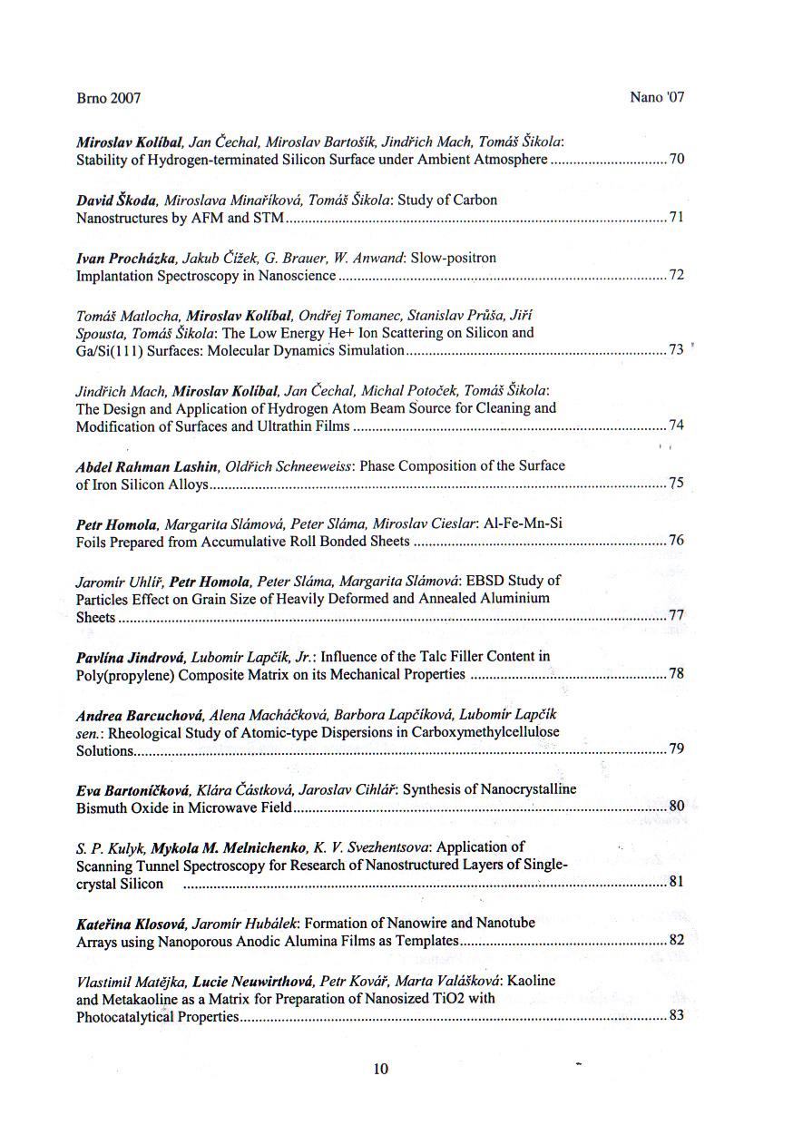
10 ULTRAFINE GRAIN STRUCTURE DEVELOPMENT IN STEELS WITH DIFFERENT CARBON CONTENT SUBJECTED TO SEVERE PLASTIC DEFORMATION Zrnik J. 1, Dobatkin S. 2, Kovarik T. 3 1 Comtes FHT, Plzen, Czech Republic, jzrnik@comtesfht.cz 2 Baikov Institute of Metalurgy and Materials Science, RAS, Moscow, Russia 3 West Bohemian University, Plzen, Czech Republic VYUŽITÍ EXTRÉMNE PLASTICKÉ DEFORMACE NA PŘÍPRAVU ULTRAJEMNÉ STRUKTURY V OCELÍCH S RŮZNYM OBSAHEM UHLÍKA Zrnik J. 1, Dobatkin S. 2, Kovarik T. 1 1 Comtes FHT, Plzeň, Česká republika, jzrnik@comtesfht.cz 2 Baikov Institute of Metalurgy and Materials Science, RAS, Moscow, Russia 3 Západočeská univerzita, Plzeň, Česká republika Abstract The article focuses on the results received from recent experimental of severe plastic deformation of low carbon (LC) and medium carbon (MC) steels performed at increased temperatures. The grain refinement of ferrite respectively ferrite-pearlite structure is described. While LC steel was deformed by ECAP die (ε = 3) with a channel angle φ = 90 the ECAP severe deformation of MC steel was conducted with die channel angle of 120 (ε = 2.6-4). The high straining in LC steel resulted in extensively elongated ferrite grains with dense dislocation network and randomly recovered and polygonized structure was observed. The small period of work hardening appeared at tensile deformation. On the other side, the warm ECAP deformation of MC steel in dependence of increased effective strain resulted in more progressive recovery process. In interior of the elongated ferrite grains the subgrain structure prevails with dislocation network. As straining increases the dynamic polygonization and recrystallization became active to form mixture of polygonized subgrain and submicrocrystalline structure. The straining and moderate ECAP temperature caused the cementite lamellae fragmentation and spheroidzation as number of passes increased. The tensile behaviour of the both steels was characterized by strength increase however the absence of strain hardening was found at low carbon steel. The favorable effect of ferrite-pearlite structure modification due straining was reason for extended work hardening period observed at MC steel. Transmission electron microscopy of thin foils revealed that three executed passes at increased temperature were not enough to form fully fine grained structure with high angle grain boundaries regardless that dynamic recrystallization advanced. The tensile behaviour of ECAP specimens was noticeably different from that of thermomechanically processed steels. ECAP processing contributed significantly to deformation behaviour of steels and affected the yield stress and ultimate tensile strength of both steels. Unfortunate polygonization process was local and heterogeneous and resulted in negligible strengthening region at both steels. Keywords: Carbon steels, ECAP processing, SEM and TEM structure analysis, recovery, polygonization, properties. Abstrakt V príspevku sú prezentované výsledky získané pri experimentu zameranom na realizáciu intenzívnej deformácie za zvýšenej teploty ocelí s nízkym (oceľ AISI 1010) a stredným (AISI 1045) obsahom uhlíka. V príspevku sú popísané štruktúrne a subštruktúrne
11 zmeny, ktoré sú výsledkom intenzívnej deformácie vo feritickej monoštruktúre a dvojfázovej feriticko-perlitickej štruktúre. Intenzívna deformácia nízkouhlíkovej ocele bola realizovaná v ECAP zápustke s uhlom kanálov φ =90, počet prechodov N=3 (efektívna deformácia ε = 3). Deformácia sa realizovala pri štyroch teplotách v rozmedzí C. Pri deformácii stredneuhlíkovej ocele pri teplote 400 C bola použitá ECAP zápustka s uhlom medzi kanálmi φ = 120 a počet prechodov bol N=4,5 a 6 (efektívna deformácia ε = 2,6-4). V dôsledku intenzívneho pretvárnenia nízkouhlíkovj ocele, bez ohľadu na teplotu deformácie, došlo k silnému pretvárneniu feritických zŕn a vytvoreniu hustej dislokačnej štruktúre, v ktorej v závislosti od teploty tvárnenia boli pozorované prejavy dynamických prejavov zotavenia a polygonizácie. V oceli s vyšším obsahom uhlíka v závislosti na veľkosti vloženej deformácie prejavy dynamických uzdravovacích a polygonizačných procesov boli výraznejšie. So zvyšovaním deformačného pretvárnenia, tj. s rastúcim počtom prechodov cez zápustku, procesy polygonizačné a prejavy rekryštalizácie boli výraznejšie, výsledkom bolo vytvorenie zmiešanej polygonizovanej a submikrokryštalickej štruktúry feritu. Proces deformácie zrn s lamelárnou štruktúrou perlitu mal zá následok fragmentáciu lamiel cementitu a ich čiastočnú sferoidizáciu a rozsah týchto zmien bol závislý na počte prechodov zápustkou. Zmena mechanických vlastností v závislosti na stupni pretvárnenia bola u oboch ocelí vyhodnotená ťahovou skúškou. U nízkouhlíkovej ocele bol pozorovaný výrazný nárast pevnostných charakteristík, ale len nepatrný úsek deformačného spevnenia. Priaznivejší efekt na deformačné chovanie, hlavne na nárast pevnostných hodnôt, ale so zachovaním plastických vlastností s ohľadom prítomnosť deformačného spevnenia, bol pozorovaný u ocele s feriticko-perlitickou štruktúrou. Deformačné chovanie obidvoch ocelí sa výrazne odlišovalo v porovnaní so stavmi ocelí, ktoré odpovedali ich normalizačnému žíhaniu. Procese intenzívnej deformácie za zvýšených teplôt inicioval uzdravovacie a polygonizačné procesy v obidvoch oceliach, ktoré v závislosti na ich rozsahu priaznivo ovplyvnili pevnostné charakteristiky, ale ich rozvoj nebol uniformný a dostatočného rozsahu, čo rezultovalo v obmedzení procesov deformačného spevnenia u oboch ocelí. 1. Introduction The fabrication of bulk materials with ultrafine grain (UFG) sizes has attracted a great deal of attention over the past two decades because of the materials enhanced properties [1-3]. UFG grained metallic materials whose grain sizes are smaller than 1µm have been actively studied as the advanced high strength materials for structural application. The conventional grain refinement of commercial steels has been achieved by thermomechanical processing using phase transformation [4]. The grain size after phase transformation is significantly smaller than of the austenite, because a number of new grains with different crystal orientations evolve within individual austenite grains during the transformation. In recent years a worldwide effort is increasing in combination of the ultra grain refinement by severe plastic deformation and the subsequent phase transformation process to fabricate ultrafine grain structures in bulk steels with submicron grains. In the past decade, various of severe plastic deformation (SPD) techniques have been used to refine structure of metals and alloys. To introduce large plastic strain into bulk material different processes like ECAP [1], high pressure torsion (HTP) [5], accumulative roll bonding (ARB) [6, 7], constrained groove pressing (CGP) [8], and others were developed and used. It is especially the ECAP that generates interest among investigators since it is one of the advanced methods of severe plastic deformation used for metallic materials to produce massive billets with ultrafine grained structure. However, UFG materials manufactured by the SPD processes have the inherent limit for their practical use. Since the SPD accumulates extensive internal energy inside materials, considerable residual stress would still remain even after a large portion of internal energy is dissipated for grain refinement.
![Very recently, significant interest has shifted to the use of warm and/or even hot severe deformation in order to produce more stable UFG microstructure [9].](/docs-images/80/82331746/images/12-0.jpg "With cold ECAP, low and medium carbon steels can only be pressed by two or three passes with channel intersection of 90 before initiation a failure of sample.")
![The two to four passes realized currently with cold ECAP are insufficient and the achievable strain amount is insufficient to produce a completely refined grain structure [10].](/docs-images/80/82331746/images/12-1.jpg "To form stable ultrafine grain structure in metals and alloys, ECAP should be carried out at the temperature corresponding to the temperature of cold working [11].")
12 Very recently, significant interest has shifted to the use of warm and/or even hot severe deformation in order to produce more stable UFG microstructure [9]. With cold ECAP, low and medium carbon steels can only be pressed by two or three passes with channel intersection of 90 before initiation a failure of sample. The two to four passes realized currently with cold ECAP are insufficient and the achievable strain amount is insufficient to produce a completely refined grain structure [10]. To form stable ultrafine grain structure in metals and alloys, ECAP should be carried out at the temperature corresponding to the temperature of cold working [11]. The purpose of this work is to study the formation of submicrocrystalline structure in low and medium carbon steels subjected to large strain during warm ECAP pressing in dependence on varying temperature and effective strain. 2. Experimental procedures In this work, two grades of commercial carbon steels with different carbon content were used for experimental. The chemical composition of both steels was as follows: low carbon steel AISI 1010, Fe- 0.1C-0.08Si-0.42Mn (in wt pct) and medium carbon steel AISI 1045,Fe-0.45C- 0.23Si-0.63Mn-0.18Cr-0.043Al. Prior to ECAP pressing, AISI 1010 billets were soaked at temperature of 920 C for 1 hour, and billet of AISI 1045 were soaked at the temperature of 960 C for 2 hours, followed by air cooling. The representative initial structures of both steels after thermal treatment, as SEM micrographs, are presented in Fig. 1 and Fig.2. From the treated plates the cylindrical billets with initial diameter of 9 mm and length of 50 mm were cut off for the ECAP experiment. The warm ECAP pressing of AISI 1010 steel was performed at two temperatures of 250 C and 300 C, respectively, and each billet was pressed up to a total of N=3 passes. The angle of intersections of the two channels φ was 90. ECA pressing yielded an effective strain ε~3. 25 µm Fig. 1. Initial ferrite structure of AISI steel with 0.1%C. 10 µm Fig. 2. Initial ferite-pearlite structure of AISI The AISI 1045 steel billets were subjected to warm ECA pressing at T= 400 C and to higher number of passes, N = 4, 5, 6 respectively. In this case the intersection angle of channels was φ = 120. Effective strain corresponding to one pass was ε ~ In both ECAP experimental the route Bc was chosen. The sample was rotated 90 around its longitudinal axis between each pass, in the same direction. The heating of sample for prior to pressing was done inside the preheated die until sample reached the pressing temperature of 300 and/or 400 C, respectively.


13 The microstructural examination of thermally treated and ECAP samples was carried out by utilizing scanning electron microscopy (SEM) and transmission electron microscopy (TEM). Thin foils for TEM observation were sliced normal to the longitudinal axis of ECAP pressed billets. The SEM and TEM micrographs were obtained by using JEOL JSM 6380 SEM operating at 10 kv and JEOL JEM 200FX TEM operating at 200 kv. Tensile test were carried out using Zwick universal testing machine equipped with Multisens extensometer. Tensile specimens with gauge length of lo= 20 mm were tested at a constant cross-head speed of mm/s until failure. The engineering stress-strain curves were constructed. 3. Experimental results and discussion 3.1. Microstructure of steel AISI The substructure of samples subjected to warm ECAP at temperature of 250 C and 300 C was investigated by TEM. Comparing effect of different ECAP temperatures, exposed to N = 3 passes no substantial difference in microstructure samples was observed. The substructure analysis provided the evidence that at the tine of structure formation not the grain fragmentation modified the newly born ultra fine substructure but also the in-situ recovery process, due to increased ECAP temperature, contributed to development of UFG structure. For the most part, the microstructure consists mainly of parallel bands of elongated, formerly equiaxed, ferrite grains, Fig. 3. The substructure modification across the cross section were detected and varied locally. High dislocation density and dislocation cells inside elongated grains are apparent. At both ECAP temperatures in some elongated ferrite grains, dislocation activities can be related to progress in polygonization and preliminary nucleation of new subgrains. As temperature of ECAP increased, the tendency for development of submicrocrystalline structure becomes stronger, which can be attributed to in-situ dynamic polygonization and recrystallization. The more grown and already equiaxed grains of high angle boundaries, with less dislocations in 400 nm 200 nm Fig. 3. TEMmicrostructure after ECAP at 150 C, N=3 Fig. 4. TEM microstructure after ECAP at 300 C, N=3. defined thick boundaries would be attributed to a recovery and recrystallization process. The presence of net pattern in SAED confirms the presence of reasonable portion of boundaries having high angles of misorientation.


14 3.2. Microstructure of steel AISI The TEM microstructures of medium carbon steel after ECAP at 400 C are presented in Fig. 5 and Fig.6. Using ECAP channel angle of 120 the structure deformation was found heterogeneous. The areas of severe deformation where cementite fragmentation and dislocation network in ferrite is evident are next to polygonized structure in deformed ferrite grains. Investigating the substructure, also the cementite lamellae spheroidization was apparent, Fig. 6. The dislocation substructure in ferrite grains was modified upon dynamic polygonization, however the subgrains with low angle boundaries are still in ferrite grains. Submicrocrystalline structure is formed within ferrite grains. As ECAP straining increases the progress in dynamic polygonization proceeded and formation of submicron size subgrains can be observed in ferrite and also between cementite plates. This observation on substructure development indicates that formation of more homogeneous submicrograined structure was not accomplished in medium carbon steel due to lower strain introduced to specimen after six resulting from ECAP angle of µm 500 µm Fig. 5. TEM microstructure of ferrite - pearlite resulted after ECAP at 400 C, N=4. Fig. 6. TEM microstructure of ferrite - Pearlite resulted after ECAP at 400 C, N= Tensile properties of AISI 1010 The results of tensile testing at room temperature are shown in Fig. 7 for ECAP specimens. In case of the fully annealed condition, there is an extensive period of strain hardening and a high elongation to failure (~30%). The similar deformation behaviour for both ECAP was observed and the tensile strength is decreasing as ECAP temperature increases. As similar to other UFG materials, the tensile deformation behaviour of the UFG low carbon steel is characterized by strength increase and absence of strain hardening region. The region of strain hardening prior the softening period is quiet short but detectable and the period of uniform elongation is moderately increasing with increasing temperature of ECAP. The decrease of the UTS can be attributed to the effective dynamic recrystallization process and formation of submicrocrystalline microstructure Tensile properties of steel AISI As concerns the deformation behaviour of the MC steel subjected to ECAP the tensile tests records are shown in Fig. 8. For all specimens there is quiet extensive region of work hardening (8-10%), after yielding, and a quiet large elongation to failure as the introduced strain was increased in dependence of ECAP passes involved. The plastic behaviour of this steel is noticeable different from that of the LC steel. At this time such deformation behaviour can be
15 attributed to existence of larger volume fraction of submicrostalline grains in the structure. The more advanced dynamic recovery and dynamic recrystallization are the processes, which actually participated in structure transformation process. Fig. 7. Engineering stress-strain curves for ECAP AISI 1010 steel. Fig. 8. Engineering stress-strain curves for ECAP AISI 1045 steel. 4. Conclusions Microstructural evolution during warm ECAP was studied in low carbon steel AISI 1010 and medium carbon steel AISI The major results can be summarised as follows: 1. Warm ECAP of low carbon steel leads to formation of heavily deformed substructure consisting of dislocation cells and subgrains. In the substructure, due to local recovery and polygonization process, areas with submicrocrystalline structure are formed. Partly recovered plastic ability caused the decrease of strength properties. 2. Microstructural observation of ECAP AISI 1045 medium carbon steel revealed the appearance of polygonized submicrocrystalline structure of high angle boundaries in large extent, which were the formed due to effective activation of dynamical recovery and polygonizational process during warm ECAP. Formation of ultrafined polygonized structure partially recovered the plasticity of ECAP steel without strength reduction. Acknowledgement This work was supported by the Ministry of Education, Youth and Sports of the Czech Republic through the Research Proposal under the contract No. MSM References [1] V.M. Segal, Mater. Sci. Eng. A, 197, 1995, p [2] R.Z. Valiev, R.K. Islamgaliev, I.V. Alexandrov, Progr. Mater. Sci., 45, 2000, p [3] R.Z. Valiev, A.V. Korznikov, R.R. Mulyukov, Fiz. Met. Metalloved. 4, 1992, p. 70. [4] [N.Tsuji, Tetsu-To-Hagane, 88 (2002) 359]. [5] R.Z. Valiev, R.K. Islamgaliev, I.V. Alexandov, Progr. Materials Sci., 45, 2000, p [6] Y. Saito, H. Utsunomiya, N. Tsuji, T. Sakai, Acta Mater., 47, 1999, p [7] N. Tsuji, R. Ueji, Y. Minamino, Scripta Mater. 47, 2002,p. 69. [8] D. H. Shin, J.J. Park, Y.S. Kim, K.T. Park, Mater.Sci. Eng. A, 375, 2002, p [9] P. De Hodgson, M.R. Hickson, R.K. Gibbs, Mater. Sci.Forum, 63-72,1998, p [10] S.V. Dobatkin, P.D. Odesski, R. Pippan, G.I. Raab,.N.A. Krasilnikov, A.M. Arsenkin, Russian Metallurgy (Metally), 1, 2004, p. 94. [11] S.V. Dobatkin, Severe Plastic Deformation of Steels: Structure, Properties and Techniques, in Investigations and Applications of Severe Plastic Deformation, Ed. by T.C. Love and R.Z. Valiev (Kluwer, Netherlands, 2000), Vol. 3/80, p
16 HIGH-TEMPERATURE DEFORMATION OF AN ECAP AA 7075 ALUMINUM ALLOY K. Turba 1, P. Málek 1,2, I. Drbohlav 3 1 Department of Physics of Materials, Faculty of Mathematics and Physics, Charles University in Prague, Czech Republic, turba@met.mff.cuni.cz 2 COMTES FHT, s.r.o., Pilsen, Czech Republic 3 Institute of Physics, Academy of Sciences of the Czech Republic, Czech Republic VYSOKOTEPLOTNÍ DEFORMACE HLINÍKOVÉ SLITINY AA 7075 PŘIPRAVENÉ METODOU ECAP K. Turba 1, P. Málek 1,2, I. Drbohlav 3 1 Katedra fyziky materiálů, Matematicko-fyzikální fakulta, Univerzita Karlova v Praze, Česká republika, turba@met.mff.cuni.cz 2 COMTES FHT, s.r.o., Plzeň, Česká republika 3 Fyzikální ústav, Akademie věd České republiky, Česká republika Abstract An ultra-fine grained microstructure was introduced into a commercial AA 7075 alloy by equal-channel angular pressing (ECAP). Three different pressing temperatures were used. The high-temperature mechanical properties of the alloy were studied using tensile tests. Strain rate change (SRC) tests were used to determine the optimum conditions with respect to eventual superplastic deformation. Consequently, tensile tests with a constant rate of crosshead displacement were performed at selected strain rates and straining temperatures. The material pressed at the highest temperature (493 K) exhibited superplastic behavior with a ductility of 370 % at 673 K and an initial strain rate of 2x10⁻³ s -1 and a ductility of 275 % at 723 K and an initial strain rate of 1x10⁻² s -1. At these conditions, the strain rate sensitivity parameter substantially exceeded the value of 0.3. The other two variants of the material remained on the verge of superplastic behavior with ductilities slightly exceeding 200 % and a strain rate sensitivity in the vicinity of 0.3 at optimum conditions. Using the methods of light microscopy and atomic force microscopy (AFM), grain boundary sliding was documented in all three variants of the material when strained at conditions which correspond to the maximum strain rate sensitivity. However, the material pressed at 493 K exhibited a greater homogeneity of grain boundary sliding and larger displacements at individual grain boundaries. Keywords: Ultra-fine grained materials, ECAP, AA 7075, superplasticity. Abstrakt Pomocí metody ECAP (úhlové protlačování s konstantním průřezem) byla v komerční hliníkové slitině AA 7075 vytvořena ultrajemnozrnná mikrostruktura. Protlačování probíhalo za třech různých teplot, čímž de facto vznikly tři varianty studovaného materiálu. Ke studiu mechanických vlastností za zvýšených teplot byly použity tahové zkoušky. Metodou náhlých změn deformační rychlosti (SRC) byly získány závislosti parametru rychlostní citlivosti napětí na skutečné deformační rychlosti pro různé teploty deformace. Na základě těchto výsledků byly vyhodnoceny optimální podmínky vzhledem k možnosti superplastické deformace. Následně byly za vybraných deformačních podmínek provedeny tahové zkoušky s konstantní rychlostí posuvu příčníku. Materiál protlačovaný při nejvyšší teplotě (493 K) vykazoval superplastické
17 chování s dosaženou tažností 370 % při 673 K a počáteční deformační rychlosti 2x10⁻³ s -1 respektive 275 % při 723 K a počáteční deformační rychlosti 1x10⁻² s -1. Za těchto deformačních podmínek parametr rychlostní citlivosti napětí výrazně překročil hodnotu 0,3. Druhé dvě varianty materiálu se pohybují na hranici superplastického chování s tažnostmi mírně převyšujícími 200 % a rychlostní citlivostí blížící se hodnotě 0,3 za optimálních podmínek deformace. Metody světelné mikroskopie a mikroskopie AFM byly využity ke studiu deformačního mechanizmu uplatňujícího se při deformačních podmínkách, které odpovídaly nejvyšším dosaženým tažnostem. U všech tří variant materiálu byl zdokumentován pokluz po hranicích zrn, nicméně materiál protlačovaný při nejvyšší teplotě, tj. 493 K, vykazoval na mezoskopické úrovní větší homogenitu deformace a zároveň větší pokluzy na jednotlivých hranicích. 1. Introduction The reduction of grain size in polycrystalline materials is known to result in an augmentation of room temperature strength and can, at the same time, promote superplastic behavior at elevated temperatures. The refinement of the microstructure can be accomplished through various procedures. It has been shown that severe plastic deformation (SPD) can be used to produce ultra-fine grained (UFG) materials, i.e. materials with grain sizes in the micrometer or sub-micrometer range. To date, equal-channel angular pressing (ECAP) [1] seems to be the most promising SPD method with respect to eventual applications in the commercial practice. Its main advantage lies in the possibility of producing large bulk samples of UFG material with no residual porosity. The objective of the present investigation was to refine the microstructure of a commercial 7 series aluminum alloy (Al-Zn-Mg-Cu) using ECAP and to study the effect of the refinement on its mechanical properties at elevated temperatures, with emphasis on the possibility of superplastic behavior. The 7 series aluminum alloys are known for their superior mechanical properties, and it is of great scientific interest to try and further enhance them using ECAP. A well established commercial alloy with no modifications except for the ECAP itself was deliberately chosen, for its more direct applicability in the industry. 2. Experimental material and procedure The studied material was a commercial AA 7075 alloy with the following composition (in wt. %): 5.88 Zn, 2.45 Mg, 1.32 Cu, 0.37 Fe, 0.35 Si, 0.19 Cr, 0.17 Mn, Ti and balance Al. The alloy was subjected to 6 passes of ECAP, using route B C and a pressing speed of 5 mm/min. The channel had a 10 x 10 mm 2 cross-section and an angle of 90. Three different pressing temperatures were used: 393, 443 and 493 K. It was thus made possible to investigate the effect of the pressing temperature on the resulting microstructure and mechanical properties of the studied material. Prior to ECAP, the alloy was annealed for 8 h at 673 K to facilitate the pressing. After ECAP, tensile specimens with a gauge length of 17 mm and a rectangular crosssection of 6 x 1 mm 2 were machined from the billets, with their tensile axis parallel to the pressing direction. Tensile tests in the temperature range of K were performed on an Instron testing machine. The method of abrupt strain rate changes (SRC) was used to obtain the dependence of the strain rate sensitivity parameter m on true strain rate for a wide range of strain rates and different deformation temperatures. These results were then used to determine the optimum straining conditions with respect to the possibility of superplastic deformation for each material. Consequently, the samples were strained to failure with a constant rate of crosshead displacement at these conditions.
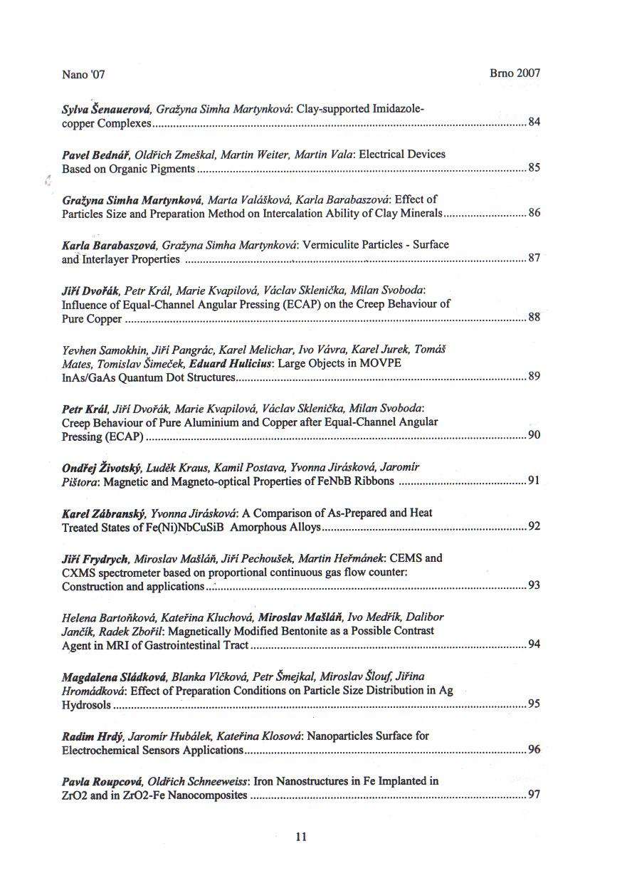
18 The methods of light microscopy (LM) and atomic force microscopy (AFM) were used to study the microstructure of the material as well as the operating deformation mechanism at selected straining conditions. Tensile samples were polished and then strained to 20 % plastic strain. The material was not etched, i.e. the necessary contrast for the LM and AFM images arose solely as a result of grain boundary sliding during the deformation. Using the method of AFM, it was possible to quantify the displacements at individual grain boundaries. 3. Experimental results The results of the strain rate change tests showed that both of the materials which had been pressed at lower temperatures exhibit a maximum strain rate sensitivity in the vicinity of 0.3. This maximum is reached at 573 K and a true strain rate of 3x10⁻³ s -1 for the material pressed at 393 K and at 1x10⁻³ s -1 and 623 K for the material pressed at 443 K respectively. Beyond these temperatures, the strain rate sensitivity of the first two variants of the material dropped significantly. On the contrary, the material which had been pressed at the highest temperature (493 K), exhibited a strain rate sensitivity substantially exceeding the value of 0.3 up to the [MPa] ECAP Al-7075 T e = 493 K 573 K 623 K m K 623 K 673 K 723 K 773 K ECAP Al-7075 T e = 493 K 523 K 573 K 673 K 723 K K 723 K K [s -1 ] [s -1 ] Fig. 1. Dependence of true stress on true strain rate for the material pressed at 493 K Fig. 2. Dependence of strain rate sensitivity on true strain rate for the material pressed at 493 K temperature of 723 K. Fig. 1 shows the dependence of true stress on true strain rate for this material at different temperatures. We can see that at 673 and 723 K, the curves exhibit sigmoidal behavior. The corresponding dependence of the strain rate sensitivity parameter m on true strain rate is presented in Fig. 2. At the temperature of 723 K, m remains above the value of 0.3 up to strain rates exceeding 1x10⁻² s -1. A strong decrease in the strain rate sensitivity and a displacement of the entire curve towards lower strain rates was recorded only at the temperature of 773 K. Fig. 3 shows the true stress vs. strain curves corresponding to the tensile tests with a constant rate of crosshead displacement. The appearance of the samples strained to failure together with an overview of the recorded ductilities is documented in Fig. 4. The highest elongation to failure % - was reached at 673 K and an initial strain rate of 2x10⁻³ s -1 in the material that had been pressed at 493 K. The same material also reached an elongation to failure of 275 % at 723 K and an initial strain rate of 1x10⁻² s -1. The sample with the largest ductility deformed in a homogeneous manner and showed little evidence of necking. Using the methods of light microscopy and AFM, grain boundary sliding (GBS) was documented in all three variants of the studied material, when strained at optimum conditions.
![[MPa] 60 ECAP AA 7075 ECAP at 393 K strained at 573 K 40 ECAP at 443 K strained at 623 K ECAP at 493 K strained at 673 K 20 ECAP at 493 K strained at 723 K 0 0 100 200 300 plast Fig. 3. Dependence of true stress on strain for materials strained to failure Fig.](/docs-images/80/82331746/images/19-0.jpg "4. Appearance of samples strained to failure at optimum conditions The two materials which had been pressed at the lower temperatures exhibited nearly identical behavior, as far as GBS is concerned.")
.")
19 [MPa] 60 ECAP AA 7075 ECAP at 393 K strained at 573 K 40 ECAP at 443 K strained at 623 K ECAP at 493 K strained at 673 K 20 ECAP at 493 K strained at 723 K plast Fig. 3. Dependence of true stress on strain for materials strained to failure Fig. 4. Appearance of samples strained to failure at optimum conditions The two materials which had been pressed at the lower temperatures exhibited nearly identical behavior, as far as GBS is concerned. As documented by Fig. 5, the homogeneity of grain boundary sliding was mediocre in spite of the fine grain size. Regions with typical dimensions of approximately 10 µm where GBS did not occur could frequently be found (the smooth areas on the micrograph). Also, the displacements at individual grain boundaries measured by AFM remained under 100 nm. Fig. 6 illustrates the microstructure of the material pressed at 493 K and then strained at 673 K. We can see that even at this temperature, the grain size remains in the order of microns and grain boundary sliding is more homogeneous than in case of the materials pressed at the lower temperatures. AFM recorded larger displacements at individual boundaries, which manifested themselves in turn by creating greater contrast on the LM images. Fig. 5. Microstructure of the material pressed at 443 K, then strained to 20 % at 623 K Light microscopy, magnification 2000 x

20 4. Discussion It is evident from the experimental results that in the case of the studied alloy, the variant which had been pressed at the highest temperature (493 K) has the best superplastic properties. At 673 and 723 K, its strain rate sensitivity substantially exceeds the value of 0.3, which, along with the sigmoidal dependence of true stress on true strain rate, represents typical characteristics of superplastic behavior [2]. This was confirmed by the achievement of superplastic ductilities at 673 and 723 K. The superplastic properties degrade only at 773 K, which is no doubt caused by the coarsening of the microstructure. It should be pointed out that the strain rate of 1x10⁻² s -1, at which the material still reached an elongation to failure of 275 %, is considered to be the lower limit for the so called high strain rate superplasticity (HSRSP) [3]. This is a very promising result with respect to the eventual applications of the studied material in the industry. Fig. 6. Microstructure of the material pressed at 493 K, then strained to 20 % at 673 K Light microscopy, magnification 2000 x The mechanical properties of the material are in accord with the LM and AFM observations. The ultra-fine grained microstructure remains reasonably stable up to the temperature of 723 K, which allows for a homogeneous distribution of grain boundary sliding and accounts for the possibility of superplastic deformation at a high strain rate. The two variants of the material which had undergone ECAP at a lower temperature remain on the verge of superplastic behavior. This is most likely caused by a larger amount of energy stored in the material after the severe plastic deformation during ECAP, which represents a higher driving force for grain growth. It can be expected that during the pressing at a higher temperature, partial dynamic recovery will lower the deformation energy stored in the material and thus make the UFG microstructure more stable. Such behavior was documented in an earlier study of a similar alloy (also AA 7075). ECAP was carried out at a lower temperature with 8 instead of 6 passes. This lead to a microstructure which was ultra-fine grained, but remained stable only up to the temperature of 573 K, with grain sizes exceeding 100 µm at 673 K [4]. On the contrary, the same alloy after thermomechanical processing but no ECAP (with a mean grain size of 13 µm) exhibited good stability at high temperatures [5]. However, it was superplastic only at 773 K and low strain rates between 10-4 and 10-3 s -1. This documents the relevance of the results in the
21 present study, where a commercial AA 7075 alloy with no further stabilizing additions exhibited superplastic behavior on the verge of high strain rate superplasticity after ECAP. 5. Conclusions I. An ultra-fine grained microstructure was introduced into a commercial AA 7075 aluminum alloy by equal-channel angular pressing (ECAP), which was carried out at 3 different pressing temperatures. II. The UFG microstructure of the material pressed at 493 K remained relatively stable at high temperatures, which promoted superplastic behavior. An elongation to failure of 370 % was reached at 673 K and an initial strain rate of 2x10⁻³ s -1. At 723 K, the material achieved a ductility of 275 % at an initial strain rate of 1x10⁻² s -1. III. The variants of the material pressed at 393 and 443 K remained on the verge of superplastic behavior with m in the vicinity of 0.3 and maximum ductilities of 215 and 240 % respectively. IV. Using the methods of light microscopy and AFM, grain boundary sliding was documented in all three of the materials. However, the material pressed at 493 K exhibited a greater homogeneity of GBS as well as larger displacements at individual boundaries. Acknowledgement This research was supported by the research goal MSM and by the Grant Agency of the Czech Republic under the grant No. 106/07/0303. The authors would also like to thank Dr. Edgar Rauch (SIMAP - GPM2, INP Grenoble) for kindly providing his ECAP facility. References [1] Segal, V. M., Reznikov, V.I., Drobyshevskij, A.E., Kopylov, V.I.: Russ. Metall 1 (1981) 99 [2] Edington, J. W., Melton, K. N., Cutler, C. P.: Progr. Mat. Sci. 21 (1976) 61 [3] Glossary of Terms used in Metallic Superplastic Materials, JIS H 7007, Japanese Standards Association, Tokyo, 1995, p. 3. [4] Málek, P., Cieslar, M.: Mater. Sci. Eng. A 324 (2002) 90 [5] Málek, P., Brázdilová, D.: Kovove Mater. 36 (1998) 42
22 DEFORMATION BEHAVIOUR OF 7075 ALUMINIUM ALLOY PROCESSED BY ECAP Lukáč P. 1,2, Turba K. 2, Málek P. 2 1 COMTES FHT, s.r.o., Pilsen, Czech Republic, lukac@met.mff.cuni.cz 2 Deparment of Physics of Materials, Faculty of Mathematics and Physics, Charles University, Praha, Czech Republic DEFORMAČNÍ CHOVÁNÍ HLINÍKOVÉ SLITINY 7075 PŘIPRAVENÉ METODOU ECAP Lukáč P. 1,2, Turba K. 2, Málek P. 2 1 COMTES FHT, s.r.o., Plzeň, Česká republika, lukac@met.mff.cuni.cz 2 Katedra fyziky materiálů, Matematicko-fyzikální fakulta, Universita Karlova, Praha, Česká republika Abstract The present paper describes the investigation of the deformation behaviour of a 7075 Al alloy prepared by equal channel angular processing (ECAP) technique. A sample was pressed through a channel (L-shaped) with a cross-section of 10 mm x 10 mm and an angle of 90. A total of six passes was performed using route B C. The ECAP processing was performed at 120, 170 and 220 ºC. Ultrafine grained materials were obtained. The ECAP-processed samples were machined to tensile specimens with their tensile axis parallel to the pressing direction. Uniaxial tensile tests were carried out in an INSTRON testing machine. The tests were conducted at temperatures between room temperature and 300 ºC at a constant crosshead speed giving an initial strain rate of 10-3 s -1. It is shown that the yield stress, estimated as the flow stress at 0.2 % strain, and the maximum stress, estimated as the maximum value of the flow stress, decrease with increasing testing temperature. The elongation to failure increases with increasing temperature. The values of the yield stress, the maximum stress (ultimate tensile stress) and the elongation to failure depend also on the ECAP processing conditions. The yield stress and the maximum stress of ECAP-processed specimens at room temperature are close to the wrought alloys but the values are higher than those of the coarse grained specimens. The specimens prepared by ECAP show an improvement of ductility in comparison to the conventional 7075 alloys that exhibit poor elongation to fracture. Keywords: Ultrafine grains, Al-Zn-Mg-Cu alloy, ECAP, deformation behaviour. Abstrakt Článek popisuje deformační chování hliníkové slitiny 7075 připravené metodou úhlového protlačování se stejným průřezem (metoda ECAP). Průřez kanálu byl čtvercový o rozměru 10 mm x 10 mm a úhel mezi vstupní a výstupní části kanálu byl 90. Protlačování vzorků proběhlo při třech různých teplotách 120, 170 a 220 C šestinásobným průchodem použitím postupu (route) B C. Byl získán ultrajemnozrnný materiál. Z takto připravených vzorků byly vyrobeny vzorky pro deformaci tak, že osa vzorku (totožná s osu namáhání) byla rovnoběžná s osou protlačování. Jednoosá tahová deformace proběhla v univerzálním zkušebním stroji typu INSTRON při konstantní rychlosti příčníku, odpovídající konstantní počáteční deformační rychlosti 10-3 s -1, v intervalu teplot mezi pokojovou teplotou a 300 C.
23 Bylo zjištěno, že mez kluzu, určena jako deformační napětí při 0,2 % deformaci, a maximální napětí, určeno jako maximální hodnota deformačního napětí, klesají s rostoucí teplotou deformace. Deformace do lomu roste s deformační teplotou. Hodnoty meze kluzu, maximálního napětí a deformace do lomu jsou závislé na podmínkách, při kterých byla použita metoda ECAP. Hodnoty meze kluzu a maximálního napětí pro protlačované vzorky (připravené metodou ECAP) deformované při pokojové teplotě jsou blízko hodnotám pro tvárné slitiny série 7075 a jsou vyšší než pro vzorky s hrubým zrnem. Deformace do lomu pro vzorky připravené metodou ECAP a deformovaných při pokojové teplotě je vyšší v porovnání s hrubozrnnými vzorky hliníkové slitiny serie 7075, které mají velmi nízkou tažnost. 1. Introduction It is well known that mechanical properties of metallic materials are very sensitive to the grain size. A reduction of the mean grain size increases the yield stress and the ultimate tensile strengths (the maximum stress) of a material at room temperature according to the Hall- Petch relationship. On the other hand, very small grains (typically about or less than 10 µm) promote superplastic properties of the material at a relatively high temperature (usually higher than 0.5 T m, where T m is the absolute melting temperature). Langdon [1,2] has shown that superplasticity is an important mode of deformation in many aluminium alloys. Suryanarayana [3] claimed that ultrafine grained materials, with grain sizes between 100 and 1000 nm have the greatest potential for industrial applications. Materials with ultrafine grain sizes may be produced by various techniques of severe plastic deformation. Among all the severe plastic techniques, processing by equal channel angular pressing (ECAP) is very often used because it yields bulk samples without any change in the cross-section of the sample and without cavities (100 % dense). The principle of ECAP is described elsewhere [4,5]. Samples subjected to ECAP usually attain homogeneous microstructure. This is important for superplastic deformation at higher temperatures and superplastic forming. Processing by ECAP produces a superplastic capability. Achieving a superplastic behaviour through ECAP has been reported for many aluminium alloys by Langdon and his co-workers (see e.g. [6,7]). The objective of this paper is to examine the deformation behaviour of Al-7075 alloy prepared by ECAP and deformed at temperatures, between 0.3 T m and 0.6 T m. 2. Experimental procedure The Al-7075 alloy with chemical composition (in mass %) of 5.88 Zn, 2.45 Mg, 1.32 Cu, 0.37 Fe, 0.35 Si, 0.19 Cr, 0.17 Mn, Ti, and the balance Al was investigated in this study. Samples with ultrafine grain sizes were produced by ECAP. The material in the soft state was prepared by annealing at 400 C for 8 h before ECAP. All samples were pressed through a die within a channel (L-shaped configuration) with a cross-section of 10 mm x 10 mm and an angle of 90 between the two parts of the channel. The samples were pressed through 6 passes using route B C the sample was rotated by 90 along their longitudinal axis in the same direction between each pass. The samples were produced at three pressing temperatures, T P : 120, 170 and 220 C with a pressing speed of 5 mm/min. The grain size was found to be between 500 and 700 nm. Tensile specimens with a gauge length of 17 mm and with a rectangular cross-section of 6 mm x 1 mm were machined from the ECAP-processed samples. The specimen tensile axis was parallel to the pressing direction. Uniaxial tensile tests were carried out in an INSTRON testing machine. The tests were performed at temperatures between room temperature and 300 ºC at a constant crosshead speed giving an initial strain rate of 10-3 s -1. The true stress, σ, and true strain, ε, were calculated using standard expressions. From the true stress true strain
24 curves, the yield stress, σ 02, and the maximum stress, σ max, were estimated as the flow stress at 0.2 % strain and as the maximum value of the flow stress, respectively. The elongation to failure, ε f was also determined. 3. Experimental results and discussion The mechanical properties of the Al-7075 alloy are shown in Table 1 after processing by ECAP at three different temperatures T P. Table 1 Mechanical properties T P = 120 C 23 C 100 C 200 C 300 C σ 02 (MPa) σ max (MPa) ε f (%) T P = 170 C σ 02 (MPa) σ max (MPa) ε f (%) T P = 220 C σ 02 (MPa) σ max (MPa) ε f (%) It is necessary to note that samples after processing at 220 ºC were deformed at 300 C to a selected strain about 10 %. Then strain rate change experiments were conducted and therefore it was not possible to estimated the maximum stress; an elongation to failure of about 100 % was observed. From Table 1 some important observation may be made. It can be seen that the mechanical properties depend very sensitively not only on the testing temperature but also on the pressing temperatures during ECAP technique. At room temperature the yield stress and maximum stress decrease with increasing pressing temperature. The values of the yield stress and maximum stress of specimens deformed at 100 C also decrease with increasing pressing temperature. The ECAP process increases the dislocation density. The dislocation strengthening has significant contribution to the strength enhancement and influences the deformation behaviour. A reduction of the strength with increasing pressing temperature may indicate a softening process during ECAP. The ECAP production leads to a reduction of the dislocation density with increasing pressing temperature owing to softening (dynamic recovery). It should be noted that complete recrystallization of the Al-7075 alloy was observed when it was annealed up to 300 C [8]. On the other hand, the yield stresses of the specimens deformed at 100 C are higher than those at room temperature for the specimens pressed at the same temperature. The reason is not clear. At 200 and 300 C, the values of the yield stress and maximum stress are lower than those for all the specimens pressed at the same pressing temperature; the elongations to failure at these temperatures are hihger. The lowest yield stress was observed for ECAP processed specimen pressed at 120 C and deformed at 200 C. An increase in the yield stress for the specimens deformed at 200 C with increasing pressing temperature may be caused by the high angle boundaries formed by ECAP. There is not any significant difference among the maximum stresses for all the specimens deformed at 200 C. The specimens deformed at 200 C exhibit elongations to fracture of about 190 % and 100 % for the pressing ECAP temperatures of 120 and 170 C. The values of the elongation to failure for
25 the specimens deformed at 300 ºC are about 200 %. It is obvious that the deformation characteristics show a non-monotonous variation with the testing temperature. The materials pressed at 120 ºC exhibit a tendency to superplastic behaviour at and above 200 ºC. The good (enhanced) tensile ductilities (the bottom limit of superplastic ductility) achieved at 200 C are usually achieved for unpressed Al alloys at higher temperatures (about C). It is apparent from inspection of Table 1 that at room temperature the specimens exhibit higher work hardening at the very beginning of deformation at lower strains. At room temperature the work hardening rate is higher than at 200 C where a steady state course of the true stress true strain curves is observed. The work hardening rate is very low, close to zero indicating the occurrence of significant strain softening. At 200 C a dynamic balance between hardening due storage of dislocations and softening owing to annealing of dislocations occurs. Grain boundary mobility should be taken into account. 4. Conclusions The results show that the ECAP temperature and testing temperature influence the deformation behaviour of the Al-7075 alloy. The specimens deformed at room temperature and 100 C show enhanced strength (the high values of the yield and maximum stress) whereas the specimens deformed at 200 C exhibit enhanced ductility (elongations to fracture of 100 % and 190 % for the specimens pressed at 170 and 120 C, respectively). The high density of dislocations produced by ECAP is responsible for the high strength. Acknowledgement This work war conducted within the framework of Research Program MSM supported by the Ministry of Education, Youth and Sport of the Czech Republic. The authors would like to thank Professor Dr. Edgar Rauch (GPM2 SIMAP, INP Grenoble) for kindly providing his ECAP equipment. References [1] Langdon, T.G.: Mater. Sci. Eng. A, vol. 137, 1991, pp [2] Langdon, T.G.: Mater. Sci. Eng. A, vol. 174, 1994, pp [3] Suryanarayana, C.: Adv. Eng. Mater., vol. 7, 2005, pp [4] Furakawa, M., Horita, Z., Langdon, T.G.: Adv. Eng. Mater., vol 3, 2001, pp [5] Langdon, T. G.: Mater. Sci. Eng. A, vol 462, 2007, pp [6] Xu, C., Furakawa, M., Horita, Z., Langdon, T.G.: Adv. Eng. Mater., vol. 5, 2003, pp [7] Balasubramanian, N., Langdon, T.G.: Mater. Sci. Eng. A, vol , 2005, pp [8] Zhao, Y.H., Liao, X.Z., Jin, Z., Valiev, R.Z., Zhu, Y.T.: Acta Mater., vol. 52, 2004, pp
26 THE ROTARY DIE EQUAL CHANNEL ANGULAR PRESSING SYSTEM Donič T.,Martikán M., Udvorka A. University of Žilina, Univerzitná 1, Žilina, Slovakia EXPERIMENTÁLNY PRETLÁČACÍ SYSTÉM ECAP-RD Donič T.,Martikán M., Udvorka A. Žilinská univerzita v Žiline, Univerzitná 1, Žilina, Slovensko Abstract This contribution is predominantly focused on design, technical drawing documentation and practical realization of experimental system for creating nanostructures in metal materials using intense shear deformation. The realized experimental system called ECAP Rotary Die is unique because of its conception and construction. The criterion of real ability to create the system based on detailed technical drawing documentation was an important criterion when choosing Rotary-Die method. Extreme requirements were put on internal and external universality of construction of system ECAP-RD especially the capability of its adaptation to three experimental load systems with special set of adjustable parameters for each of them which consequently determine parameters of experiment and differentiate each other by method of inducing stresses in specimen. Great attention was put to the strength calculations of functional parts of ECAP-RD experimental system because of ability to select the most suitable materials for these parts and heat treatment of these parts which are exposed to high temperature and highstress conditions at the same time. Further the heating system which is capable of generating heat sufficient to heat up specimens up to 700 C and which is the separate part of ECAP-RD is presented as well. After processing the specimens by ECAP-RD system the various tests were conducted on them including tensile tests, compress tests, evaluation of coefficient of thermal expansion and poisson ratio value (by ultrasonic method) etc. But that is not subject of this paper. Keywords: Nanostructure, ECAP, Rotary Die Abstract Príspevok je prevažne zameraný na dizajn, technickú dokumentáciu a praktickú realizáciu experimentálneho systému pre tvorbu nanoštruktúr v kovových materiáloch použitím intenzívnej šmykovej deformácie. Realizovaný experimentálny systém nazývaný ECAP RD (rotary die) je jedinečný vo svojej koncepcii a konštrukcii. Výroba systému ECAP RD vyžadovala precíznosť vo vytváraní jeho funkčných častí a teda hlavným kritériom pri konštrukčnom návrhu systému bolo kritérium reálnej vyrobiteľnosti celého experimentálneho zariadenia. Vysoké požiadavky boli kladené na vnútornú a vonkajšiu univerzálnosť konštrukcie systému ECAP-RD a to hlavne schopnosť jeho adaptácia do troch rôznych experimentálnych zaťažovacích systémov pričom každý má špeciálny súbor nastaviteľných parametrov, ktoré priamo určujú aj parametre samotného experimentu, a ktoré sa líšia navzájom metódou vyvolávania napätí vo vzorke. Veľká pozornosť bola venovaná pevnostným výpočtom jednotlivých funkčných častí experimentálneho nástroja z dôvodu schopnosti vybrať najvhodnejšie materiály pre tieto časti a tepelné spracovanie týchto častí, ktoré sú vystavené vysokej teplote a veľkým napäťovým zaťaženiam v rovnakom čase. Ďalej je prezentovaný ohrievací systém, ktorý je konštruovaný ako separátna časť systému RD-ECAP, a ktorý je schopný generovať teplo postačujúce na ohriatie vzorky až na teplotu 700 C. Po procese pretláčania v systéme ECAP-RD boli vzkonané na vzorkách rôzne testy vrátane ťahových skúšiek, kompresných skúšiek, stanovenia coeficientu tepelnej rozťažnosti a hodnoti
.")

27 poissonového čísla (ultrazvukovou metódou) a ďaľšie. Ale tieto nie sú priamo predmetom tohoto príspevku a teda tu nie sú ani prezentované. 1. Introduction The criterion of real ability to make the system based on detailed technical drawing documentation was an important criterion when choosing Rotary Die method (Fig.1). Extreme requirements were put on internal and external universality of construction of system ECAP. Fig. 1 Process sequence of rotary-die equal-channel angular pressing. [1] 1.1. Construction of RD-ECAP experimental system Great attention was devoted to strength calculations of functional parts of experimental system ECAP Rotary Die (Fig.2), to selection of construction materials and their refining. Fig. 2 Computer models of particular parts of RD-ECAP system Presented system ECAP Rotary Die (Fig.3, Fig.4) in this scope and details has not been published yet.


28 Fig. 3 Core of RD-ECAP system Fig. 4 Assembly of whole RD-ECAP system

, which is an independent part of system ECAP Rotary Die. Fig.")

29 Procedures of using this system, including procedures of manipulating with samples, and also disassembly and assembly of the experimental system itself, are identified in the contribution in detail. With great attention were treated also systems of heating samples up to 700 C using the heating module (Fig. 5), which is an independent part of system ECAP Rotary Die. Fig. 5 Heating system for RD-ECAP experiments conducted at elevated temperatures As mentioned above the RD-ECAP tool was designed with respect to requirements on its universality particularly possibility of implementation into three experimental load systems - HECKERT, HILTI (Fig. 6a, b) and CAM Plastometer (Fig.7), which in themselves are characterized by different mechanisms of induced strength deformation effect, i.e. statics and dynamics. a) b) Fig. 6 System HECKERT a) and system HILTI b)
. a) b) Fig.")


30 Fig.7 system CAM Plastometer Experimental verification of functionality of ECAP Rotary Die system was performed on compacts of aluminium powder 99.9% with particle size of 1 µm (Fig.8a, b). a) b) Fig. 8 Precompacted aluminium powder specimens a) and specimen after forward extrusion process b) ECAP process is supported by substantial photo documentation which in detail identifies zones (Fig. 9) of deformed powder compact under slip plane in the area of most intense shear deformations and also in the zone, in which, while maintaining the original cross section of the sample, it does not come to plastic deformations. 500x magnified images the most that used optical system Olympus allowed, are presented. Zones where intense plastic deformation disrupted oxidic layers on the basic aluminium matrix, which subsequently allowed realization of diffusion processes in the main aluminium monocrystalic matrix were identified.

31 Fig. 9 Metallography of specimen after RD-ECAP Conclusion The making of system ECAP Rotary Die required excellent precision in making functional parts of the deformation system. After forward extrusion process, which supplied specimens for RD-ECAP experiments, the grain size of compacts is higher than initial size of aluminium powder particles what is caused by diffusion process between individual powder particles. Presumption that during ECAP process the grain size of aluminium specimens prepared by forward extrusion of fine aluminium powder decreases, was confirmed. Acknowledgement The contribution was made with support from grant agency APVV of Slovak Republic for science research assignment APVV with the name of: Creation of nanostructures in metal materials using intense plastic deformations and their relation to physical mechanical properties. Literature [1] Ma A., et al.: Characteristics of plastic deformation by rotary-die equal-channel angular pressing. Scripta Materialia 52 (2005)
32 MATHEMATICAL SIMULATION AND EXPERIMENTS OF ECAP Kvačkaj T. 1, Kočiško R. 1, Besterci M 2., Pokorný I 1., Kuskulič 1 T., Sülleiová K 2., Molnárová M 1., Kováčová A., Slabeyciusova S 3., Donič T 3. 1 Technical University in Košice, MF-DMF, Letná 9, Košice, Slovakia 2 Institute of Materials Research, SAS, Košice, Slovakia 3 University of Žilina, ME-DAM, Žilina, Slovakia MATEMATICKÉ SIMULÁCIE A EXPERIMENTY PRE ECAP Kvačkaj T. 1, Kočiško R. 1, Besterci M 2., Pokorný I 1., Kuskulič 1 T., Sülleiová K 2., Molnárová M 1., Kováčová A., Slabeyciusova S 3., Donič T 3. 1 Technická univerzita v Košiciach,HF-KTK,Letná 9, Košice, Slovensko 2 Ústav materiálového výskumu SAV, Slovensko 3 Žilinská univerzita v Žiline, SjF, KAM, Žilina, Slovensko Abstract Equal channel angular pressing (ECAP) is a material processing method for developing an ultrafine-grained (UFG) structure by introducing severe plastic deformation in a bulk material with no changes in its cross-section. Numerous analytical and numerical studies on equal channel angular pressing have been performed in recent years. The present work focuses on the effects of die geometry width is defined by the angle between two channels Φ, angle on outer corner of die Ψ (or radius R) and angle within internal corner (or radius r) of die on medium effective strain after one pass route. Next, there are analyses of strength properties, plastic properties, fracture mechanism, as well as analyses of Cu structure evolution after severe plastic deformations (SPD) by ECAP technology, in the paper. The sixteen passes through the ECAP matrix were realized using route C. The following experimental results and their analyses, the biggest increase of strength and microhardness was prooved already after 4th pass. Valuation of fracture surfaces shows that after 12th pass plastic fracture is transformed to transcrystalics. Final average (middle) grain size was analyzed by TEM and AFM method. After 4th pass, the middle grain size decreased from initial approximate size 7 μm to 200 nm, whereby the average grain size was changeless after subsequent deformations. Possible mechanism of high-angle boundary nanograins evolution consists of formation of cell structure, subgrains that transform with the increase of deformation into nanograins with big-angle misorientation. Keywords: equal-channel angular pressing (ECAP), finite element method, severe plastic deformation, ultra-fine grained materials Abstrakt Uhlové pretlačovanie cez kanál rovnakého prierezu (Equal Channel Angular Pressing ) je spracovateľská metóda kovov, pre vytváranie ultrajemných štruktúr pomocou intenzívnych plastických deformácii (Severe Plastic Deformations), bez zmeny v priečnom priereze vzorky. V posledných rokoch bolo na ECAP vykonaných mnoho analytických a numerických štúdii. Táto práca sa sústreďuje na vplyv geometrie ECAP nástroja, ktorý je definovaný uhlom medzi dvoma kanálmi Φ, vonkajším R a vnútorným r rádiusom kanála na hodnotu strednej efektívnej deformácie po prvom prechode. Ďalej, v práci sú analyzované pevnostné a plastické vlastnosti, lomový mechanizmus, ako aj vývoj mikroštruktúry Cu vzorky deformovanej intenzívnymi plastickými deformáciami (SPD) technológiou ECAP. Bolo realizovaných šestnásť prechodov

33 cez ECAP matricu, cestou C. Na základe experimentálnych výsledkov a ich analýz bol preukázaný najväčší nárast pevnosti a mikrotvrdosti už po štvrtom prechode. Hodnotenie lomových plôch ukázalo, že po dvanástom prechode je tvárny lom transkryštalický. Výsledná stredná veľkosť zŕn bola analyzovaná pomocou TEM a AFM metódy. Po štvrtom prechode stredná veľkosť zŕn klesla z východiskovej veľkosti cca 7 μm na 200 nm, pričom po následných deformáciách sa stredná veľkosť zŕn nemenila. Pravdepodobný mechanizmus tvorby veľkouhlových nanozŕn spočíva vo formovaní bunkovej štruktúry, tvorbe subzŕn, ktoré sa s rastom deformácie postupne transformujú do nanozŕn s veľkouhlovou dezorientáciou. 1. Introduction Present scientific research is intensive centred on ultra-fine grained structures formation (UFG with grain diameter 1μm 30 nm), and nanoscale structures (NSG with grain diameter 30nm) in polyedric metallic materials, attained through the use of severe plastic deformations (SPD). Attaining this grain size dimensions represent not only the necessity of scientific problems solution in partial areas like physical metallurgy, construction of machinery for SPD, tribology etc., but also knowledge synthesis leading to industrial use of materials with definite mechanical properties. UFG materials produced by SPD are characterized by increased value of strength, elongation, fatigue properties and superplasticity. Attaining these properties is dependent on nanoscaled structure, its distribution in material, stresses, texture and other structure properties. Even though the scientific research of nanoscaled structures formation by SPD started in 1981, when authors [1] published the possibility of UFG formation by SPD for the first time, there are still scientific questions focused on research of mechanisms leading to their formation. Authors [2] draw attention to important fact that structure evolution during SPD is unrelated with subsequent microstructure refinement, but has a relation with transformation of dislocation substructure to ultra-fine structure with big-angle grain boundary. Nanostructured materials are, after [3, 4], plastic deformed by taking part of dislocation slips, or dislocations rotation inside grains and slips evolution at grain boundary, at ambient temperature. Various plastic deformation processes have been designed for processing materials using simple shear. One of these techniques is equal channel angular pressing (ECAP) originally designed by Segal [5]. Shearing strain depends on geometry of ECAP instrument, that is defined by the angle between two channels Φ, angle on outer corner of die Ψ (or radius R) and angle within internal corner (or radius r) of die. Various combinations can occur in the process of ECAP between transformed parameter of die R, r for single angles Φ. Design of ECAP die, if 0 R π-φ a r 0 is shown Fig.1. For this case Peréz [6] have derived an equation Eq.1 for shearing strain. Effective strain after N cycles by Von Misses s criterion is introduced by the relationship Eq.2. specime n x/2 R π-φ r Φ Fig. 1 Design of ECAP matrix, where 0 R π-φ and r 0. x sin x 2 2.cot. 2 2 x x cos.sin n N. 3 (1) (2)
34 flow stress This paper deals with structures classification attained by SPD, influence of ECAP channel geometry on plastic deformation intensity and on Cu substructure evolution after ECAP process. 2. Clasification of structures according to Hall-Petch equation One of nanocrystaline materials deformation processes specific feature is the deviation from known equation for grain size. Classic Hall-Petch equation [7, 8] is about relation between yield strength R e and grain size d in polycrystalline materials: Re Re0 k d n (3) where: R e0 lattice friction stress, for dislocations motion, k slope of a straight line, called Hall-Petch slope, dependent on material, n exponent. Experimental analyses of Hall-Petch equation for different metals show three different areas, Fig.2 [9]: - relevance of Hall-Petch equation is in the range from monocrystal to grain size of 1μm, whereby exponent n has enduring value from -0,5 to 1, - Hall-Petch equation is relevant, i.e. increase of yield strength occurs with decrease of grain size, but not so intensive as in previous case, whereby exponent n < -0,5; equation is relevant in grain size range from 1μm to 30 nm, - Hall-Petch equation loses its relevance, i.e. with the decrease of grain size the decrease of yield strength occurs; i.e. slope of straight line change occurs, exponent can change its value, whereby grain size is 30nm and has extremely high volume value of grain boundaries over 50%. grain size [-] ~ 1 m 30 m 10 nm coarse grain ultrafine grain nanosize grain grain size [-] -1/2 Fig.2. Structures classification At present, the nature of the deviations from the conventional Hall-Petch grain size scaling relation in nanocrystalline materials is the subject of controversy. In general, theoretical models of the phenomenon discussed can be divided into the two basic categories: a) models describing nanocrystalline materials as two-phase composites with grain interiors and boundaries playing the role as component phases; b) models describing evolution of defects and grain boundary structures, with focuses placed on physical mechanisms (lattice dislocation motion, grain boundary sliding, diffusion plasticity mechanisms) of plastic flow in nanocrystalline materials. The models of category (a) operate with the averaged mechanical characteristics and volume fractions of the graininterior and grain-boundary phases. The models of the category (b) deal with the nano-scale effects on conventional lattice motion and the competition between various deformation mechanisms and the effects of a distribution of grain size on this competition in nanocrystalline materials.
35 2. Experimental material and methods As experimental material, the high pure Cu (99,99%) was used. Initial mechanical properties and grain size of pure Cu are in Tab. 1. Tab. 1 Cu properties before ECAP R p 0.2 [MPa] R m [MPa] A 5 [%] Z [%] HV d z [μm] , Specimen with dimensions Ф 10 x 70 mm was extruded through the use of ECAP technology, with matrix channel angle Ф=90. The ECAP process was realized by hydraulic press with max. force of approximately 1 MN. Sixteen ECAP passes were realized using route C. Next the specimens for static tensile test, microhardness and metallographic analysis (microstructure, substructure by TEM and AFM) were made from extruded experimental material. Mathematical simulations of ECAP process were made for the purpose of reviewing the outer and inner radius influence on middle deformation intensity ε equ.m for angles Ф=90, 100, 110 a 120, after the 1st pass. These simulations were realized by software product DEFORM, with respect for work hardening of experimental material. 3. Results and discussion Middle deformation intensity ε equ.m was measured in cross-section of samples, i.e. in steady state of plastic deformation, as it is on Fig. 3. Mathematical simulations made for the purpose of reviewing the influence of ECAP matrix channel angle on evolution of effective deformation showed that, the highest effective deformation value is attained at angle Ф=90, whereby with increase of angle Ф the effective deformation decreases [10, 11], as it is shown on Fig.4. Results from these graphs show, that middle deformation intensity for channel angles Ф = 90 a 100 decreases with the increase of outer and decrease if inner radius; and for channel angles Ф = 110 a 120 the average (middle) deformation intensity decreases with the increase of inner and outer radius. Sample end Steady state Initial Cu structure is coarse grained, with average grain size 7 μm and low yield strength and tensile strength, but with sharply defined reduction of area (82%). Cold plastic deformation leads to increase of strength properties. The biggest increase of yield strength and tensile strength can be seen after the 4th ECAP pass, as it is shown on Fig. 5. Mild decrease of strength properties can be seen after the 14th ECAP pass. Change of microhardness HV10 shown in Fig.6 has a similar character as R p0,2, R m, where after the 14th pass clear decrease of microhardness occurs. Elongation after Fig.7 was changeless during the 16 ECAP passes, but on the other hand area reduction as more sensitive to plasticity evaluation (for local deformation in neck area) confirmed the structure, or substructure change after the 14th pass. This change can be attributed to change of plastic deformation mechanism, which cause Hall-Petch equation inversion. Initial material grain shape is polygonal and uniform. After successive deformations of 2, 4, 14 and 16 passes, there is a decrease of grain size. Despite the sample rotation during plastic deformation, grain structure is uneven and partly elongated in direction of deformation with predomination of big-angle boundaries. Insufficient structure homogeneity will have negative influence mostly on properties stability, whereby evident changes of mechanical Measurement area Sample front Fig. 3 Distribution of deformation intensity ε in cross-section of sample.
36 Elongation - A [%] Reduction of area - Z [%] Elongation - A [%] Reduction of area - Z [%] Yield strength - R p0,2 [MPa] Yield strength - R p0,2 [MPa] Tensile strength - R m [MPa] Tensile strength - R m [MPa] Microhardness - HV 10 Microhardness - HV [-] 1 [-] R [mm] R [mm] r [mm] Ф=90 r [mm] Ф= [-] 0.66 [-] R [mm] Ф= r [mm] R [mm] Ф=120 4 r [mm] 2 0 Fig. 4 Influence of R and r on middle deformation intensity ε equ.m, in cross-section of sample Rp0,2 Rp0,2 [MPa] [MPa] Rm Rm [MPa] [MPa] No. No. of of ECAP ECAP passes passes [-] [-] Dependence Dependence of of mechanical mechanical properties properties on on ECAP ECAP passes passes (Material: 99,99% Cu) (Material: 99,99% Cu) Fig. 5 Dependence of R p0,2 and R m on ECAP passes HV HV No. No. of of ECAP ECAP passes passes [-] [-] Dependence Dependence of of microhardness microhardness on on ECAP ECAP passes passes (Material: 99,99% Cu) (Material: 99,99% Cu) Fig. 6 Dependence of HV10 on ECAP passes A A [%] [%] Z Z [%] [%] No. No. of of ECAP ECAP passes passes [-] [-] Dependence Dependence of of plastic plastic properties properties on on ECAP ECAP passes passes (Material: 99,99% Cu) (Material: 99,99% Cu) Fig. 7 Dependence of A and Z on ECAP passes

![disorientation, as it is indication in [12]. Next method used for evaluation of average subgrain size was AFM. The Fig.](/docs-images/80/82331746/images/37-1.jpg "8 shown topography Cu 99,99% after 12th pass and plane cut average nanograin size is in the range of 100-300nm, whereby average nanograin diameter is d z = 200nm. a) b) Fig.")
37 properties ensure only big-angle grain boundaries. From TEM analyses can be seen, that average grain size after the 10th ECAP pass is in the range nm. Possible mechanism for evolution of big-angle nanoscaled grains consists of formation of cell structure, subgrains which transform with deformation increase to nanograins with big-angle disorientation, as it is indication in [12]. Next method used for evaluation of average subgrain size was AFM. The Fig. 8 shown topography Cu 99,99% after 12th pass and plane cut average nanograin size is in the range of nm, whereby average nanograin diameter is d z = 200nm. a) b) Fig. 8 Topographic scan of ultrafine structure after 10th ECAP passes CONCLUSION From mathematical simulations and experimental results we can draw following conclusions: - optimal radius for different angles were derived from point of view homogeneity of plastic deformation in sample cross-section - mechanical properties growth up to the 4th pass intensively and fall down after the 12th pass - valuation of fracture surfaces showed, that after the 12th pass plastic fracture is transformed to transcrystalics - initial grain size before ECAP was dz~7 mm, after the 12th pass dz~200 nm and after the 14th dz~ 200nm - TEM analysis showed on possibility of nanostructure formation mechanism by cellular structure formation in grain, forming of subgrains and then forming of high angle nanograins with random orientation LITERATÚRA: [1] Segal V. M., et al: Izvestia AN ZSSR, Metally, 1981, No.1, p. 115 [2] Rybin V.V.: Boľšie plastičeskie deformacii i razrušenie metallov, Moskva, Metallurgija, 1986 [3] Gertsman V. Ju., et al: Material Science Forum, 1996, vol. 233, p. 80 [4] Ovidko I. A.:Rev. Adv. Scie., 10, 2005, p. 89 [5] Segal V.M.: Mater. Sci. Eng. A 197 (1995) p.157 [6] Luis Perez C.J.: Scripta Materialia 50 (2004),p. 387 [7] Hall E.O.: Proc. Phys. Soc. London B 64 (1951) p.747 [8] Petch N.J.: J. Iron Steel Inst. 174 (1953) p.25 [9] Gutkin M. Y., Ovid ko I. A., Pande C. S.: Rev.Adv.Mater.Sci. 2 (2001) p. 80 [10] Kvačkaj T., et al: NANOVED, máj, (2006), Stará Lesná, Slovakia, poster [11] Kočiško R., et al:acta Metallurgica Slovaca, 13, 2007, p. 397 [12] Besterci M., et al: First Afro-Asian Conference on Advanced Materials Science and Technology, Nov , Cairo, Egypt, p. 42
38 NEW ASPECTS OF ECAP PROCESS SIMULATIONS Rusz, S 1., Malaník, K. 2 1 Department of Mechanical Technology, Faculty of Mechanical Engineering, VSB TU Ostrava, Czech Republic, stanislav.rusz@vsb.cz 2 VUHZ Dobra, a. s., Dobra, Czech Republic, malanik@vuhz.cz NOVÉ POZNATKY ZE SIMULACE PROCESU ECAP Rusz, S 1., Malaník, K. 2 K katedra mechanické technologie, VŠB TU Ostrava, Česká Republika,stanislav.rusz@vsb.cz 2 VÚHŽ Dobrá, a. s., Dobrá, Česká Republika, malanik@vuhz.cz Abstract The principle of the ECAP (Equal Channel Angular Pressed) technology has been known since the nineties of the past century. Nevertheless concrete utilizations of this technology for ultra-fine material structure developments have been rather rare. This paper informs on ECAP technology investigations that have been oriented by overall objectives of acquiring new knowledge concerning deformation resistances, stress condition impacts, and physical/technological conditions as decisive factors of material formability processes that provide for ultra-fine sized grain structures of very good mechanical properties and good plasticity. The investigation principal goal consisted in analyzing of the ECAP technology mathematical simulation concerning AlCu4Mg2 alloy sample extruded by passing through channels of different radii of inner and outer walls, R1 = 4 mm, R2 = 0.2 mm, and constant channel width 10x10 mm. The axis offset of horizontal part of the channel by 10 and 20 in horizontal direction is a completely new structural design which substantially increases efficiency of the ECAP process. During the next stage of research works computer simulation of the first pass was made for the same alloy AlCu4Mg2. Simulation was realized by program Superforge and QForm. Deflection of the channel in horizontal direction was 10 and 20. It will be necessary to optimize the given angle of deflection for various types of materials. In our case we have achieved at very small deflection rather substantial increase of deformation intensity in comparison with the case of classical shape of channel with identical angles of the channel = 90, = 90. It was unequivocally proved that axis offset of the channel makes it possible to achieve much higher amounts of deformation during the first pass through the channel of the ECAP tool, which leads to quicker refining of structure. Thanks to this cumulative effect it is thus possible to reduce number of passes leading to obtaining the required mean size of grain and therefore to make the ECAP method more efficient. Keywords: Finite element method, mathematical simulation, severe plastic deformation, intensity of stress, ultra fine structure, grain size, ECAP method, technological process. Abstrakt Principy technologie ECAP (protlačování pravoúhlým rovnostranným kanálem) jsou znány od devadesátých let minulého století. Přesto konkrétní využití dané technologie pro vývoj materiálů s velmi jemnozrnnou strukturou je poměrně malé. Daný příspěvek je zaměřen na
39 vývoj ECAP technologie, souhrnně nabyté nové informace jako jsou deformační odpor, napěťový stav, fyzikálně-technologické podmínky a další rozhodující faktory tvářecího procesu umožňující vytvoření velmi jemnozrnné struktury s vysokými mechanickými vlastnostmi a dobrou tvářitelností. Výzkum byl zaměřen na matematické modelování procesu ECAP slitiny AlCu4Mg2 protlačovanou rovnostranným kanálem s vnějším poloměrem zaoblení kanálu R1 = 4 mm a vnitřním poloměrem R2 = 0.2 mm s konstantním průřezem kanálu 10 x10 mm. Dále byl simulováno protlačování výše uvedené slitiny kanálem s vyosením v jeho horizontální části o 10 a 20. Dosahujeme daleko vyššího zjemnění struktury zvýšení efektivity procesu ECAP. V průběhu další etapy byl analyzován deformačně-napěťový stav v prvním průchodu nástrojem ECAP pomocí programu Superforge a QForm pro slitinu AlCu4Mg2.Vychýlení kanálu v horizontální ose dosahovalo hodnoty 10 a 20. Dané vychýlení je potřebné z hlediska optimalizace úhlu vychýlení pro různé typy materiálů. V našem případě jsme obdrželi významný nárůst intenzity deformace oproti klasickému konstrukčnímu řešení s úhly = 90, = 90. Dané vychýlení kanálu umožnilo dosáhnout daleko vyšší nárůst intenzity deformace v prvním průchodu nástrojem ECAP,které umožňuje dosažení vyššího zjemnění struktury. V důsledku tohoto kumulativního efektu je možno dosáhnout snížení počtu průchodů nástrojem ECAP a zároveň dosáhnout potřebné velikosti zrna (velmi jemnozrnná struktura) a tímto podstatně zefektivnit proces ECAP. Klíčová slova: Metoda konečných prvků, matematická simulace, intenzivní deformace, intenzita napětí, ultra jemná struktura, velikost zrna, metoda ECAP, technologický proces. 1. Introduction Contemporary technical progress requires development of new manufacturing technologies, which are brought as a result of development of new materials, but also due to optimisation of productivity as such. Development of new technologies aimed at production of materials with ultra-fine grained structure is at present intensively investigated in important scientific institutes and universities. Semi-products with this structure are characterised by very high mechanical properties with preservation of very good formability. Technology of multiple plastic deformation, i.e. Equal Channel Angular Pressing (hereinafter ECAP) enables achievement of high amount of deformation. Final result consists of achievement of ultra-fine grained structure. This process is known already since 1980 and its final application progressively gets into technical practice. Basic concept of use of the ECAP method is based on new findings about resistance to deformation, influence of state of stress on material plasticity. Solution will result in deepening of our knowledge about deformation behaviour of metallic ultra-fine grained materials (nano-materials) and about impact of plastic deformation on structure, mechanical properties and formability. Technology ECAP makes it possible to obtain ultra-fine grain in larger volumes, when cross section remains constant during the pressing itself. These materials are used particularly in automotive industry, as well as in military and space industry. Semi-products manufactured by this technology can be further processed into final shape e.g. by technology of super-plastic forming (Ti and Mg alloys, etc.). The products produced by the ECAP technology can be characterised by specific properties. When these materials are used in conditions defined in advance it is possible to increase requirements to their properties, or to influence the properties by development of suitable structure obtained by forming. On the basis of final requirements it is possible to modify the nano-structure and optimum mechanical properties can be obtained by optimisation of
40 forming parameters so that the products ensure for specific purpose exploitation reliability and safety. 2. Mathematic simulation o forming processes The both geometry verification of the tool and of the forming process by mathematical modelling with use of finite element method is of great importance. At present the results of experiment are not confirmed unequivocally by suitable mathematical model that would sufficiently describe these problems. Program with 2D graphics is sufficient for understanding the ECAP process after the first pass. An analysis of problems related to several passes requires simulation in a 3D space. In terms of calculation the software should be an open system with possibility of a loop check of the calculation made by the chosen method. The following software products were chosen for mathematical modelling of the process ECAP with multiple passes and for designing of the tool: MSC.SuperForm and MSC.SuperForge from the company MSC Software and also QForm 3D from the company Quantor Ltd. QForm 3D This is the newest program of the company Quantor Ltd. It is determined for simulation and analysis of forming processes in a 3D environment. System environment is similar to that of the program QForm 2D. This similarity enables natural transition between 2D and 3D simulation. Geometric objects are imported via QDRAFT 3D modules, which are also known already from the QForm 2D. QForm 3D is a perfect tool for simulation of hot and cold forming. During animation of the forming process the program QForm 3D shows material flow and also flow of generated defects [1]. Simulation also displays temperature in every part of the component and amount of deformation. A mesh is formed in the formed component. Its complexity depends on required accuracy of simulation. Results of simulation are shown by 3D graphics simultaneously with progress of simulation, which provides an immediate feedback in program SuperForge & SuperForm This program was introduced to the market by the company MSC Software. MSC.SuperForge is very strong tool for a 3D simulation of forming processes. It is successfully used for analyses of processes of bulk forming. It can be used efficiently for evaluation of influence of characteristic conditions of the forming process on material flow and on final shape and properties of the formed component [2]. Simulation is in this program based on the finite volume element method (VEM). The program MSC.SuperForge was developed on the basis of the Euler mesh, which is applied on the surface containing triangle facets. These facets are geometric entities, which serve for reading of the material surface. After application of the mesh and subsequent forming the mesh is not applied anymore, and therefore results are not distorted, which is great advantage of this program [2]. The program comprises also graphical editor, which enables specification of the shape of investigated component and tool. The program can also be linked to other graphical programs, such as ProEngineer, SolidWorks, etc. The program MSC.SuperForge serves for solution of forming processes with changing boundary conditions. 2. Principle of the ECAP process The principle of the ECAP method consists in pressing of either cylindrical or prismatic specimen through the channel of defined geometry. In an ideal case the specimen is subjected during the passage through the channel to pure shear straining. Various amounts of deformation can be obtained by selecting various angles of the corner. The most frequently used angle of the
![channel varies between 90 to 135 [3,4].](/docs-images/80/82331746/images/41-2.jpg "The tool was designed with two perpendicular channels in cross section which intersects the angle and also additional angle, which defines the angle of the curve arch at section of two channels.")

41 channel varies between 90 to 135 [3,4]. The tool was designed with two perpendicular channels in cross section which intersects the angle and also additional angle, which defines the angle of the curve arch at section of two channels. Test specimen has been adapted in such a manner that it abuts in the channel and it is pressed by the load F is exerted by the extruding punch (see Fig. 1). For achievement of the required structure the most important role is played primarily by the already mentioned tool geometry, number of passes through the tool, amount and speed of deformation, process temperature and lubrication conditions. PUNCH Specimen ECAP DIE Fig. 1 Principle of ECAP technology: illustration of shear deformation plane and working angles Due to the fact that area of the specimen cross section remains during passage through the tool unchanged at individual places, it is obvious that repeated extrusion is performed in order to obtain very high amount of deformation. In practice the specimen can be rotated between individual extrusions, which is activates different shearing system. At present four different types of passage through the channel are generally known. They are described as passage of the type A, B A, B C and type C (see Fig.2). During passage of the type A the specimen is extruded without its subsequent rotation, in case of the passage B the specimen is rotated by 90 between each extrusion with change of direction of the passage, known as the type B A, or with rotation with preservation of direction of the passage, known as the type B C. In case of passage of the type C, the specimen is rotated by 180 between each extrusion. Route A Route B C Route C Fig. 2. Main types of passage through the tool ECAP
42 2.1 Materials used of simulation of the process ECAP in the programs SuperForm and QForm Material of the tool Material Dievar, which is used for experiments at the VSB-TU Ostrava was chosen for both tools. Dievar is Cr-Mo-V alloyed high-strength steel for hot work. It is highly resistant to formation of small fissure and larger cracks due to thermal and it has also high resistance to hot wear. Material Dievar belongs to steels with the highest toughness and ductility in all directions, high resistance to tempering, high hot strength, very good hardenability, high dimensional stability at heat treatment and application of coatings. However, for simulation we have used the material SKD61 according to the Japanese standard JIS G (from the database of the program SuperForm), which was the nearest possible equivalent to the material Dievar. Material of specimens Material used for experiments at the VŠB-TUO is an aluminium alloy AlCu4Mg2, the chemical composition of which is based on the standard ČSN The alloy is hardenable with high strength and after annealing it is suitable for cold forming. It is used for various structural purposes, namely for transport vehicles and also as fastening material. Tab. 1 Chemical composition of material AlCu4Mg2 element Cu Mg Al ( % ) Tab. 2 Physical properties of material AlCu4Mg2 PROPERTY UNITS VALUES Ultimate strength Rm [MPa] max. 100 Min. ductility A10 [-] 25 Young s modulus E [MPa] 10-3 Temperature coefficient [ 1/ 0C] 20/100 Specific gravity [kg.m-3] Temperature of drawing [0C] 657 Test according to Brinel [HB] Simulation of the ECAP process was made with use of the specimen with parameters 38 mm. 10 mm x
![Calculation of achieved average value of strain rate d d t dl l d l dl dt v l [s -1 ] (1) Entry parameters: v..0.5 mm.](/docs-images/80/82331746/images/43-0.jpg "s -1 hk l 38 mm v l 0,5 38 0,013 s 1 (2) The calculation has confirmed theoretical presumption that average strain rate for the given alloy at the ECAP process varies within the range = (1.")


43 Calculation of achieved average value of strain rate d d t dl l d l dl dt v l [s -1 ] (1) Entry parameters: v..0.5 mm.s -1 hk l 38 mm v l 0,5 38 0,013 s 1 (2) The calculation has confirmed theoretical presumption that average strain rate for the given alloy at the ECAP process varies within the range = ( s -1 to s -1 ). After specification of material it is necessary to choose and define geometry of semiproduct for extrusion tests. It is also important to create a semi-product only for one of extrusion possibilities, since the programs SuperForm and QForm make it possible to take over and use the specimen with obtained parameters after the previous operation. Next step consisted of creation of tools. The tools have at simulation a simple shape that was created in the program Inventor. Pre-defined material from the program database was assigned to the tools together with initial temperatures and mesh. After that it was possible to create a set for the given operation, assignment of contact conditions, movements, movement actions and simulation could therefore be started. 3. Evaluation of results of simulation The results were evaluated with use of two programs - SuperForm and QForm, which work in a 3D environment. At spatial forming, alike as in reality, material is heterogeneous and it does not behave along its full cross section in a constant manner. Deformation intensity is at the specimen edge much bigger as it is caused by friction between the tool and the specimen. Results of simulation are therefore graphically represented in 50 % of the specimen cross section. a) b) Fig. 3 Comparison of deformation intensity in the program SuperForm a) edge of specimen, b) cross section at 50 %
44 Deformation intensity Comparison of deformation intensity for the radii R1 = 5.5 mm, R2 = 0.2 mm, with tool angles = 90 and = 90 in the program SuperForm proved unequivocally that at the edge of the specimen where it contacts the tool (see Fig. 3a) the zone of deformation is distinctly higher than at cross section at the half of the specimen width after extrusion (see Fig. 3 b) with identical value of deformation intensity i = Heterogeneity of deformation distribution in the volume of the specimen is well visible. For this reason it is necessary to limit the influence of friction between the channel walls and material and also to make several passes through the tool. 3.1 Parameters of deformation-stress state of the alloy AlCu4Mg2 at one and several passes through the ECAP channel At this stage the main objective was analysis of mathematical modelling of the ECAP technology for the specimen AlCu4Mg2, extruded through the matrix with various radii of matrix curvature R1 and R2 with constant width of the channel b = 10 mm. This dimension is not valid for the channel width between connection of its vertical and horizontal parts marked as b1 (see Fig. 4). Keeping the channel width constant requires that centres of passages must depart from one point. Adherence to this condition creates big passages of the tool channel. These parameters of the tool geometry must be preserved also in case of greater number of passages (outer and inner radii and angles), in order to ensure identical conditions of extrusion (see Fig. 4). Range of values of radii of curvatures and angles of the ECAP channel was optimised for the alloy AlCu4Mg2 with use of the program MathCad. R1 = (5.5; 2.4 and 1.85) mm, R2 = 0.2 mm, = 90 and 105, = 90 and 60 Fig. 4 Geometry of the ECAP channel outer radius R1, inner radius R2, channel width b, channel width between the curvature b1 3.2 Pass of the type C Deformation intensity For the radii R1 = 5.5 mm, R2 = 0.2 mm, with tool angles = 90 and = 90 the deformation intensity acquires the maximum value i 1 after the first pass through the tool, and the value i 1.6 after the second pass through the tool. Courses of deformation intensity are shown in the Fig. 5 a, b.


45 a) b) Fig. 5 Courses of deformation intensity a) for channel radii R1 = 5.5 mm, R2 = 0.2 mm, after the first pass b) for channel radii R1 = 5.5 mm, R2 = 0.2 mm, after the second pass 3.3 Mathematical modelling of the passage of the type B C, in the program QForm This type of pass seems to be the most suitable according to the findings obtained until now and also according to experimental verifications. The specimen is rotated between each pass by 90 in the same direction (see Fig. 6 a, b). Shear zones are cumulated in whole volume of the extruded specimen. Intensive plastic deformation obtained by high amount of deformation leads to considerable fragmentation of grains. This type of passage requires for obtaining of the same magnitude of deformation the smallest number of extrusions. This process, when the specimen is rotated in the sequence 90, 180, 270, 360, etc. marked as the passage of the type B C has manifested itself at detailed investigation of microstructure as an optimum process for obtaining of small grain size with high angles of grain boundaries. a) b) Fig. 6 Courses of deformation intensity after the first pass through the channel a) for channel radii R1 = 2.4 mm, R2 = 0.2 mm b) for channel radii R1 = 5.5 mm, R2 = 0.2 mm


46 Deformation intensity a) b) Fig. 7 Courses of deformation intensity after the second pass through the channel a) for channel radii R1 = 2.4 mm, R2 = 0.2 mm b) for channel radii R1 = 5.5 mm, R2 = 0.2 mm Deformation intensity for the radii R1 = 2.4 mm, R2 = 0.2 mm and tool angles = 90, = 90 achieves after the first pass the maximum value i Deformation intensity for the radii R1 = 5.5 mm, R2 = 0.2 mm, with tool angles = 90 and = 90 achieves after the first passage the maximum value i 1. The inner radius R2 = 0.2 mm is identical for both channels. Courses of deformation intensity are shown in Fig. 6 a, b. Reduction of the outer radius leads to increase of deformation approx. by 15%. After the second pass through the tool with radii R1 = 2.4 mm, R2 = 0.2 mm, with tool angles = 90 and = 90 the deformation intensity achieves the maximum value i 2. The value of deformation intensity for the radii R1 = 5.5 mm and R2 = 0,2 mm, with tool angles = 90 and = 90 achieves after the second pass through the tool the maximum value i 1.8. The inner radius R2 = 0.2 mm is identical for both channels (see Fig.7 a, b). Reduction of curvature of the outer channel R1 leads to increase of deformation intensity. 3.4 Influence of number of passes on obtained amount of deformation This part of works was concentrated on comparison of obtained partial results from the viewpoint of definition of tool geometry, and comparison of suitability of type of passage for achieving the highest possible amount of deformation. The same values of channel angles = 90 and = 90 are valid for compared results. The inner radius R2 = 0.2 mm is also identical.
47 Table 3 Obtained results of deformation intensity Value of radius R1 [mm] Type of passage Number of passes Deformation intensity [-] 5.5 C C B C B C B C B C The amount of deformation achieved at the second pass at the route type B C is more efficient by 12.5 % in comparison to the route C after the second pass for the angles = 90, = 90 and radii R1 = 5.5 mm and R2 = 0.2 mm. Magnitude of deformation is influenced primarily by the outer radius of curvature of the channel passage R1. In case of parameters of the channel angle = 90, angle of the outer curvature = 90, ( = ) with radii R1 = 2.4 mm and R2 = 0.2 mm the deformation intensity after the second pass was at the route B C higher by 11.1 % in comparison with the same passage, but with the parameters of angles = 90, = 90 and tool radii R1 = 5.5 mm and R2 = 0.2 mm. Influence of reduction of the outer radius on increase in deformation intensity was unequivocally proved. It has been proved from the courses of magnitude of deformation intensity that the values i are at the second pass through the tool higher than the values after the first pass. According to resulting parameters strain hardening accumulates after individual passes. Each extrusion leads to considerable refining of the average grain size. It seems that good prerequisite for obtaining the higher amount of material deformation is modification of the deformation route, which is analysed below. The main objective of this stage consisted in an analysis of mathematical modelling of the first pass through the ECAP tool channel with changed geometry of the tool. Design of new geometry of the tool should bring increase of the amount of deformation at the first pass through the ECAP tool channel due to modified deformation route. Reduction of number of passes through the ECAP tool in comparison with classical solution is very important factor from the viewpoint of development of this technology and its future in semi-industrial practice. Engineering design has the axis of the output part of the extrusion tool offset by 20. The axis of the horizontal channel of the tool is offset by 20 (see Fig. 8), and the output part has at the end of the channel slight recess at the axis y for enabling easier handling of the deformed specimen.

48 a) b) Fig. 8 ECAP tool with offset of the output part axis by 20 a) top view, b) 3D view Deformation intensity Fig. 9 Courses of deformation intensity after the first pass - SuperForm Resulting value of deformation intensity for the tool of offset of the output part axis by 10, radii of curvature R1 = 4 mm (the radius was increased due to design considerations), R2 = 0.5 mm, R5 = 5 mm and tool angles = 90, = 90 achieves the maximum value i 1.4 (program SuperForm). The course of deformation intensity is shown in the Fig. 9. It is obvious from obtained results that axis offset has substantial influence on achieved values of the amount of deformation i - increase by up to 40 % at the first pass through the ECAP tool channel in comparison with the classical design. It is completely new finding, which may substantially increase efficiency of the extrusion process. In a similar manner an axis offset of 10 was simulated. Deformation intensity i achieved the value 1.25 (increase by 25% in comparison with classical design). Comparison of achieved values of deformation intensity both for classical design and for individual angles is summarised in the Table 4.
49 Table 4 Achieved values of deformation intensity Axis offset at the channel Deformation intensity i [-] output part [ ] , ,4 The same values of channel angles = 90 and = 90 are valid for compared results. The outer radius R1 = 4 mm, inner radius R2 = 0.5 mm and radius of curvature of passage between the inclined channel and straight channel R5 = 5 mm both from its outer and inner part. Overall evaluation of performed simulations The first part of works analysed applicability of the software for simulation of the ECAP technology. Both programs, i.e. SuperForm and QForm proved good. Afterwards analyses were aimed particularly at obtained magnitudes of deformation intensity i, which influences the most the process of the grain fragmentation and obtaining of the required very fine grained structure in the least possible number of passes through the extrusion tool. Classical engineering design with 1 st and 2 nd pass through the tool was analysed. Completely new concept of axis offset at the ECAP tool output part along its full length was then analysed. The basic objective consisted in achieving of high deformation intensity in extruded specimen at the first pass through the channel. Optimisation of geometry of inner radius of the tool will be the important factor of future development, as it influences the resulting magnitude of deformation in extruded specimen and therefore also amount of the grain fragmentation, as well as homogeneity of the final structure. Designing of the new ECAP tool in comparison with the classical tools will also be rather difficult. The main problems is preservation of unchanged geometry of the channel due to high amounts of deformation and forming pressures generated at this process. Our future research, based on experimental works, will be aimed in this direction. Acknowledgement Supported by project of Ministry of Trade and Commerce of Czech Republic Trvalá prosperita č. 2A-1TP/124 References [1] QUANTOR LTD. QForm3D software, Overview [online], [2] MSC.SOFTWARE. SuperForge, Overview [online]. Last revision 2005 [ ] < [3] HEBESBERGER, Th. - VOHAUER, A. - WADSAK, R. - STÚWE, H. P. - PIPPAN, R. Production, structure and properties of nanocrystalline materials, 2002, Jg. 147, pp [4] HORITA, Z. FURUKAWA, M. NEMOTO, M. - LANGDON, T. G. Development of fine grained structures using severe plastic deformation, Materials Science and Technology, pp
50 MULTISCALE MODELLING OF NANOINDENTATION TEST IN NICKEL CRYSTAL Horníková J. a, Buršíková V. b, Šandera P. a, Černý M. a and Pokluda J. a a Brno University of Technology, Technická 2, CZ Brno, Czech Republic b Masaryk University, Kotlářská 2, CZ Brno, Czech Republic hornikova@fme.vutbr.cz, vilma.bursikova@gmail.com, sandera@fme.vutbr.cz, cerny.m@fme.vutbr.cz, pokluda@fme.vutbr.cz VÍCEÚROVŇOVÉ MODELOVÁNÍ ZKOUŠKY NANOTVRDOSTI V KRYSTALU NIKLU Horníková J. a, Buršíková V. b, Šandera P. a, Černý M. a a Pokluda J. a Vysoké učení technické v Brně, Technická 2,61669 Brno, Česká republika b Masarykova univerzita, Kotlářská 2, Brno, Česká republika hornikova@fme.vutbr.cz, vilma.bursikova@gmail.com, sandera@fme.vutbr.cz, cerny.m@fme.vutbr.cz, pokluda@fme.vutbr.cz Abstract The nanoindentation test in the dislocation free crystal of nickel is simulated by nonlinear elastic finite element analysis coupled with both ab initio calculations of the ideal shear strength and crystallographic considerations. The onset of microplasticity, associated with the pop-in effect identified in experimental nanoindentation tests (creation of first dislocations), is assumed to be related to the moment of achieving the value of the ideal shear strength for the nickel crystal. The calculated value of the related indentation load lies within the range of experimentally observed pop-ins in the nickel crystal. Keywords: Nanoindentation; Ab initio calculation; Ideal shear strength; Nickel crystal; FEM analysis. Abstrakt Zkouška nanotvrdosti v bezdislokační oblasti krystalu niklu je simulována nelineární elastickou analýzou při užití metody konečných prvků, doplněnou prvoprincipiálními výpočty ideální smykové pevnosti a krystalografickými úvahami. Počátek mikroplastického chování krystalu, spojeného s emisí dislokací, experimentálně zjišťovaného v průběhu měření nanotvrdosti, je považován za okamžik dosažení ideální smykové pevnosti pro krystal niklu. Vypočtené hodnoty nanoindentační síly leží v intervalu experimentálně pozorovaných nestabilit v krystalu niklu. 1. Introduction Nanoindentation is considered to be a very promising experimental approach to measuring the ideal shear strength since the stressed volume beneath the sharp indenter may be defect-free. The local shear component of the stress reaches its maximum value some close distance from the indenter in the bulk. The value of the stress can be near the ideal shear strength id (ISS) and, consequently, high enough to nucleate dislocations [1,2]. This process might be detected as a pop-in on the nanoindentation load-displacement curve. Indeed, some authors already reported such behaviour and tried to compare the related stress to the
51 theoretically determined ideal shear stress [3]. A relevant model of the nanoindentation test must be based on coupling of approaches on three different levels: (i) Atomistic (calculation of ISS); (ii) mesoscopic (crystallography); (iii) macroscopic (finite element analysis of stress-strain response). As a rule, however, the experimental values of the pop-in deformation lie substantially above the values obtained by majority of recent models. The reasons for that discrepancy may have several origins. First, the simple theory must be modified in order to reflect the real stress state at the point of maximum shear under the indenter. In particular, the influence of the compressive normal load on the slip plane is to be considered in the ab initio analysis. Second, a solution reflecting a three-dimensionality of the nanoindentation test is to be obtained since the stress state under the indenter must be strongly different from the two-dimensional one mostly used in recent analysis. Third, the nonlinearity in the stress-strain relation is to be taken into account. Forth, a correction is needed in order to match the orientation of the appropriate crystallographic plane, i.e. to meet the actual resolved shear stress. Fifth, the anisotropy of the elastic response of the crystal is to be considered. Sixth, friction forces between the surfaces of the substrate and the indenter should be also included into the model. The authors of the model [3] claim that all the above mentioned corrections were considered in their analysis. However, no detailed descriptions of related procedures are reported in this paper. Therefore, the relevancy of these results remains rather questionable. In the previous work [4], the first two corrections were included in the model. As a result, the theoretical values obtained lie at the lower limit of the range of experimental pop-ins. In this paper both the third and the forth corrections (the nonlinearity and the crystallography) are fully taken into account. Moreover, the influence of anisotropy is also partially included by respecting the [001] loading direction. 2. Description of the model The three-dimensional isotropic FEM analysis was performed by using the finite element ANSYS code. A frictionless sphero-conical indenter with the radius of 0.2 m in agreement with the experiment is pressed into a 5 m thick substrate disc with the radius of 10 m (see Fig. 1). In the vicinity of the interface, the sphere is meshed with elements approximately 0.2 nm and the mesh of the substrate is refined from 0.4 m at the outer edge of the disc to 0.2 nm directly beneath the indenter. The size of the elements near the contact is an order magnitude smaller in comparison to the depth of penetration (see Fig. 2). Owing to the axial symmetry of the indentation model, only 2D section could be analyzed as depicted in Fig. 2. The nonlinearity and, to a certain extent, also the anisotropy of the stress-strain elastic response was taken into account by a multilinear approximation of the stress-strain curve calculated ab initio for the [001] uniaxial tension-compression of the nickel crystal [5]. This curve was utilized in the Ansys code procedure [6] as equivalent stress-strain dependence. The Young modulus E of the indenter was taken to be of 1141 GPa and the Poisson ratio 0.07 (diamond). The dependence of id on the superimposed normal stress n is nearly linear and can be simply parameterized as s, (1) id id,0 n where id,0 corresponds to the theoretical shear strength without superimposed normal stress and the s parameter describes slope of the linear regression line. The details of the calculation procedure can be found elsewhere [4,7]. The dependence (1) for the nickel crystal is displayed in Fig. 3.
 Scheme of the tip of the diamond sphero-conical indenter with the semi-angle o 68 and the tip radius r 200nm. Fig.")
52 Fig.1: The geometrical configuration of the model. a) Cross-section of the nanoindenter and the substrate disc. b) Scheme of the tip of the diamond sphero-conical indenter with the semi-angle o 68 and the tip radius r 200nm. Fig. 2: An example of the finite element network near the contact boundary.
53 Fig. 3: The dependence (1) for the nickel crystal. The global procedure simulates, step by step, the penetration of the indenter into the nickel crystal. In order to identify the appropriate crystallographic plane in which the condition (1) for the dislocation emission is firstly reached, the activity in the slip system was considered in the calculations. With regard to the cylindrical symmetry of the solution, the stress tensor transformation was performed to obtain all possible positions of the crystallographic systems rotating according to the main coordinate system. This rotation enables us to compute the values of and as functions of the angle. Consequently, the maximum of the ratio i i id, i n is searched on the whole circle going through each node. The highest value of that ratio over all nodes and all angles is denoted as max. This value is related to the step characterised by the depth h of the penetration. 3. Results and discussion The values of max in dependence on the penetration depth h are depicted in the Fig. 4. When the value of max exceeds 1, the condition for the dislocation emission is safely fulfilled. This corresponds to the depth h 5.5nm. The situation in Fig. 4 corresponds to the calculated indentation load of 35 N and to the indenter displacement of 5.5 nm. These values are to be comparable with experimentally observed pop-ins of about 40 N and 4 nm (see Fig. 5).
54 Fig. 4: Dependence of the parameter max on the penetration depth h. The predicted moment of the first emission of dislocation loops corresponds to exceeding the critical value max 1 for h 5.5nm. Fig. 5: Experimental curves obtained by the nanoindentation in the nickel crystal to clear pop-ins (yields can be seen near the load of 40 N and the depth of 4 nm).
55 While the calculated indentation load agrees well with the experiment, the computed displacement is somewhat higher. The good agreement between the calculated and the experimental loads means that the nanoindentation provides a very good tool for measuring the ideal shear strength. This statement was also proved in case of recently modelled indentation test in the copper crystal [8]. 4. Conclusion The nanoindentation test in the dislocation free crystal of nickel was simulated by utilizing a multiscale analysis. The onset of microplasticity, associated with the pop-in effect identified in experimental nanoindentation tests (creation of first dislocation loops), is assumed to be related to the moment when the value of the ideal shear strength for the nickel crystal was reached. In particular, the influence of the compressive normal load on the slip plane, the threedimensionality of the nanoindentation test, the nonlinearity in the stress-strain relation, the orientation of relevant crystallographic planes and the anisotropy of the elastic response of the crystal were considered in the model. While the calculated indentation load agrees well with the experiment, the computed displacement is somewhat higher. The good agreement between the calculated and the experimental loads reveals that the nanoindentation test can yield sufficiently precise values for the ideal shear strength. Acknowledgement This research was supported by European agency COST (Action P19) and the Ministry of Education and Youth of the Czech Republic under the grant No. OC 148 and by the Czech Science Foundation under the project No. GA106/05/0274. References [1] Y. L. Chiu and A. H. W. Ngan: Acta Mater. Vol. 50 (2002), p [2] M. Göken, M. Kempf and W. D. Nix: Acta Mater. Vol. 49 (2001), p [3] C. R. Krenn, D. Roundy, M. L. Cohen, D. C. Chrzan and J. W. Morris, Jr.: Phys. Rev. B Vol. 65 (2002), p [4] J. Horníková, M. Černý, P. Šandera and J. Pokluda: Key Engng. Mater. Vols (2007), p [5] P. Šesták, M. Černý and J. Pokluda: Mater. Sci. Eng., in press, doi: /1.msea [6] ANSYS Users Manual. Revision 5.0, I-IV. Swanson Analysis System, Houston, USA, [7] M. Černý and J. Pokluda: Mater. Sci. Eng., in press, doi: /1.msea [8] J. Horníková, P. Šandera, M. Černý, and J. Pokluda: Engng. Fract. Mechanics (accepted).
56 MICROMAGNETIC SIMULATION OF FERROMAGNETIC NANOSTRUCTURES Voves J. Department of Microelectronics, FEE,The Czech Technical University in Prague, Czech Republic, MICROMAGNETICKÉ SIMULACE FEROMAGNETICKÝCH NANOSTRUCTUR Voves J. Katedra mikroelektroniky, FEL, České vysoké učení technické v Praze, Česká republika Abstract The semiconductor ferromagnetic layers are the perspective materials for the spintronic applications. The best results are produced on the patterned structures with nanometric constrictions. We present the simulation of the influence of the lateral confinement on the transport properties of holes in thin ferromagnetic (GaMn)As layers in the presence of the external magnetic field. Two samples are studied. The first nanostructure is the GaMnAs layer with two nanometric constrictions prepared by atomic force microscopy (AFM) lithography using the local anodic oxidation (LAO) in our laboratory. The second example is the structure with two (Ga,Mn)As nanobars, oriented perpendicular to each other and connected be the very thin neck, described in the recent publication [1]. Analysis of these structures in the external magnetic field with different orientation was performed by means of micromagnetic simulation software SimulMag [2]. This simulator minimizes the Gibbs free energy of the micromagnetic system and uses semi-empirical models for giant magnetoresistence (GMR) and anisotropic magnetoresistence (AMR) calculations. The static calculations of the resulting structure magnetisation were performed. Qualitative semi-empirical values of GMR and AMR of the first structure are presented. The dependence of the resistance on the polar orientation of the external field is calculated for the second structure. The results show, that the micromagnetic simulation by the program SimulMag can be used for the qualitative estimation of the ferromagnetic nanostructure behavior. Low temperature magnetotransport experiments are prepared for the further analysis of the ferromagnetic nanostructures and for the comparison with the simulated results. Keywords: ferromagnetic semiconductor, local anodic oxidation, atomic force microscopy, micromagnetic simulation, giant magnetoresistance, anisotropic magnetoresistance Abstrakt Polovodičové feromagnetické vrstvy jsou perspektivním materiálem pro spintronické aplikace. Nejlepších výsledků je dosahováno u litograficky opracovaných vzorků se zúženími nanometrových rozměru. V příspěvku jsou prezentovány simulace vlivu laterálního omezení na transportní vlastnosti tenkých feromagnetických vrstev (GaMn)As za přítomnosti vnějšího magnetického pole. Studovány jsou dva vzorky. První je struktura vrstvy (GaMn)As se dvěma nanometrovými zúženími připravená litografií AFM pomocí lokální anodické oxidace v naší laboratoři. Druhým příkladem je struktura se dvěma (GaMn)As nanotyčkami kolmo na sebe orientovanými, propojenými velmi tenkým krčkem, nedávno popsaná v publikaci [1]. Analýza těchto struktur za přítomnosti vnějšího magnetického pole různých orientací byla provedena pomocí mikromagnetického simulačního programu SimulMag [2], Tento simulátor minimalizuje
57 Gibbsovu volnou energii mikromagnetického systému a používá semiempirické modely pro výpočty GMR a AMR. Byly provedeny statické výpočty výsledné magnetizace struktur. U první struktury jsou prezentovány semiempirické hodnoty GMR a AMR. U druhé struktury je vypočtena závislost odporu na polární orientaci aplikovaného vnějšího magnetického pole. Výsledky ukazují, že je možné využít mikromagnetickou simulaci pomocí programu SimulMag pro kvalitativní odhad chování feromagnetických nanostruktur. Jsou připravena nízkoteplotní měření magnetotransportu pro další studium feromagnetických nanostruktur a pro porovnání s výsledky simulací. 1. Introduction Interesting spin-valve effects have been reported recently in the ferromagnetic nanostructures with the domain-wall pinning on the nanoconstrictions. The giant magnetoresistance (GMR) up to several hundred % is produced by the opposite magnetisation of adjacent domain walls, the tunnel magnetoresistance (TMR) appears, when the constrictions are very narrow (sub 10 nm), producing TMR up to several thousand %. Tunneling anisotropic magnetoresistance (TAMR) is present in the nanoconstricted structures with the strong spinorbit coupling. Application of the external magnetic field in the different directions produces both positive and negative MR. All these effects have to be analyzed theoretically and experimentally. A micromagnetic simulator is a useful tool for this purpose. Micromagnetic modeling can predict the magnetic behavior of materials on a short length scales of the order of nanometers. Individual magnetic moments will want to align with an external field, until the local energy minimum is reached. If the external field changes, the moments will rotate and the domain patterns change and move to a new configuration, corresponding to the new local energy minimum. The main focus of micromagnetism is to study the magnetization reversal process and the complex domain configurations, especially in thin films. A micromagnetic simulator is designed to compute the local magnetization within a material. The user provides inputs such as the material geometry, the initial magnetization, and the time evolution of the external magnetic field. It is also necessary to specify several parameters such as magnetization, the exchange interaction, and anisotropy for each different material. The exchange interaction field is a field between neighboring electron spins, which wants to align them to each other. Anisotropy represents a preferred direction of magnetization, which is usually in the direction of one or more of the major axes of the crystal lattice. Several free available micromagnetic simulators are available freely on the Internet. We present two examples of the static micromagnetic simulation by means of the program Simulmag [2]. Both structures are prepared by lithographic patterning of thin GaMnAs layer. The first is the quantum wire with two constrictions, prepared by the AFM lithography, the second is the structure consisting by two rectangular oriented nanobars prepared by the electron lithography. 2. Models The micromagnetic Simulator SimulMag is an easy-to-use PC-based magnetic design tool. The simulator allows one to simulate the system response of a magnetic device or circuit under the influence of external magnetic fields, currents, or local field sources. The analysis is based on a collection of single-domain elements whose size and position can be specified by the designer. The elements may be magnetic or nonmagnetic, a conductor, or an insulator. The element s magnetic properties, such as magnetization, anisotropy, pinning fields, and resistivity must be specified or selected from a library of materials. Electrical circuits can be specified and currents applied. The elements interact through magnetostatic interactions and userspecified
58 exchange interactions. The elements are arranged in groups to allow different structures to be built up and manipulated independently. Relative motion between the groups can be specified. Two types of calculation methods, one a static method and the other dynamic, are implemented for determining the equilibrium magnetization M of the elements of a system. The static method is an energy minimization calculation in which an energy minimum is calculated for a given value of applied magnetic fields. Total energy of the system we can define as integration of all components of the energy density [3]: E ( w w w w dv (1) tot exch ani ext dem) V The exchange interaction field H represents short-range exchange interactions exch between magnetic elements. Exchange interaction has a quantum-mechanical origin. The field expression used by the software is based on an energy that is formally derived from the quantum-mechanical formulation by replacing atomic-spin dot products by dot products of the magnetization vectors. The exchange interaction promotes the parallel orientation of the magnetization vectors of two coupled elements if they are ferromagnetically coupled to each other, or the antiparallel orientation of their magnetization vectors if they are antiferromagnetically coupled. A is the exchange constant: 2A 2 wexch Hexch.M, Hexch M (2) 2 M The uniaxial magnetic anisotropy field represents the first-order uniaxial magnetic anisotropy of the element and is given by the following expression where K 1 and K 2 are the magnetocrystalline anisotropy constants and θ is an angle between the magnetisation vector and the anisotropy (easy) axis: 2 4 w ani K 1 sin ( ) K sin ( ) (3) 2 The pinning field represents a unidirectional anisotropy that may be present in an element due to a variety of causes. It promotes the orientation of the magnetization vector in the pinning field direction. A popular practical example of the existence of a pinning field is the pinning of the magnetization of one of the thin-film layers of a magnetoresistive spin valve by an adjacent antiferromagnetic layer. The pinning field is a constant field term in the total field acting on the element. The external field H produces the change in the energy, known as Zeeman effect: ext w M (4) ext H ext Currents excited by external current sources produce magnetic fields that affect the magnetic state of the system as well. These are long-range fields. The field is calculated by considering subdivisions of source elements into rectangular rod-like segments in the direction of current. The demagnetizing field H is the dipolar field generated by all the microscopic dem dipoles. It follows from the Maxwell equation: 0.( H dem M) 0 (5) 1 w dem Hdem M 2 N M M (6) 2 where N is the demagnetisation tensor, depending of the structure geometry.
 where γ is the gyromagnetic ratio, α is the damping coefficient and: 1 Etot H (8) eff 0 M 3.")
As nanobars, oriented perpendicular to each other and connected be the very thin neck, described in the recent publication [2]. 3.1.")

59 The dynamic calculation is based on the Landau-Lifshitz equation and entails finding the magnetic state corresponding to the vanishing of the torque at all elements of the system: dm M Heff M M Heff dt M S (7) where γ is the gyromagnetic ratio, α is the damping coefficient and: 1 Etot H (8) eff 0 M 3. Results The first simulated nanostructure is the GaMnAs layer with two nanometric constrictions prepared by atomic force microscopy (AFM) lithography using the local anodic oxidation (LAO) in our laboratory. The second example is the structure with two (Ga,Mn)As nanobars, oriented perpendicular to each other and connected be the very thin neck, described in the recent publication [2] GaMnAs Wire with Two Nanoconstrictions We used a 10 nm thick (Ga,Mn)As layer grown on a GaAs substrate by the lowtemperature molecular beam epitaxy. The field was changed from 30 mt to -30 mt and back. The result of the LAO is shown on the Fig.1. The tip set point was lowered to 40 % of original value, increasing the force applied on the tip. Humidity was kept approximately 75%. Tip velocity during LAO was 400 nm/s. Negative bias applied on the tip was 10 V. Three parallel lines with different length can produce quantum dot separated from contacts by two Fig. 1 The AFM picture of the structure with two constrictions. The rectangle shows the simulated area. Dotted lines are the paths of the tip. Fig. 2 The input structure for micromagnetic simulation with the coordinate orientation. nanoconstrictions. Three dimensional nanostructure with two constrictions was approximated by the rectangle shaped oxide regions (Fig. 2) We performed the static calculation of the structure magnetisation. Saturated magnetisation of the central quantum dot was chosen higher (40kA/m) than in other regions (20 ka/m) to simulate the retarded switching of the central part
60 magnetisation during the magnetic field sweep. The resulting magnetisation of the sample shows different levels of hysteresis with the different field orientations (Fig. 3). Zero values of azimuth and polar angles correspond to hard axis of the sample. The hysteresis loops show several nonlinearities due to retarded domain switching of the central dot by the magnetic field change. These nonlinearities produce the sharp GMR and AMR changes, as shown in the Fig.4 and Fig GaMnAs Perpendicular Nanobars The second structure is comprised of two (Ga,Mn)As nanobars, oriented perpendicular to each other as shown in the Fig. 6. Each nanobar exhibits strong uniaxial magnetic anisotropy due to inhomogenous strain induced by the geometry of nanobars. These two nanobars are electrically connected through a constriction whose resistance is determined by the relative magnetization states of the nanobars. The anisotropic magnetoresistance effect yields different constriction resistances depending on the relative orientation of the two nanobarmagnetization vectors. The structure can thus be viewed as the basis of a ferromagnetic semiconductor memory device that operates in the non-volatile regime. The simulation has been performed for the rectangular orientation of the bars with the dimensions 1000 nm x 200 nm. The uniaxial anisotropy axis has been oriented along the long side of the bars. Width of the neck was 10 nm. Thickness of the GaMnAs layer was 10 nm. The magnetic field was changed from 0 to 30 ka/m and back with the different polar orientation. Resulting polar dependence of the sample resistivity are inverse to the dependence presented in [1] for the nanometric constriction in the neck. The behavior Fig. 3 Results of micromagnetic simulation by the external magnetic field. of the structure with two constrictions.the field was changed from 30 mt to -30 mt and back. Resulting magnetisation of the sample shows different levels of hysteresis with different field orientations. Inset shows the external magnetic field orientations - polar and azimuth angle. Fig. 4 Qualitative semi-empirical values of GMR of the structure with two nanoconstrictions. Fig. 5 Qualitative semi-empirical values of AMR of the structure with two nanoconstrictions.
, which has opposite sign in the resistance change.")
61 corresponds to the measured resistivity of the sample with the constriction width of several tens nanometers. Results presented in [1] are explained by the tunneling anisotropic magnetoresistance effect (TAMR), which has opposite sign in the resistance change. This effect is not yet included in the SimulMag model. 4. Conclusions The micromagnetic simulation can be used for the qualitative estimation of the ferromagnetic nanostructure behavior. Some effects, such as TAMR should be included in the model. The comparison of the simulated results with low temperature magnetotransport measurements of patterned ferromagnetic nanostructures is necessary for the model improvement and it will be performed soon. Fig. 6 The SEM picture of the structure with two nanobars [1] Acknowledgement The work was supported by the grant No. 102/06/0381 GACR, by the grant No. KAN GA CAS and by the grant No. MSM The Ministry of Education CR. Fig. 7 Polar graph of the resulting resistivity of the nanoconsriction between two nanobars after switching on and off the magnetic field with the different polar orientation. References [1] Pappert K., Hümpfner S., Gould C., Wenisch J., Brunner K., Schmidt G., and Molenkamp L.W.: Exploiting Locally Imposed Anisotropies in (Ga,Mn)As: a Non-volatile Memory Device, Nature Physics advance online publication, 1 July 2007 (DOI /nphys652); cond-mat/ [2] Oti J. O.: Simulmag User s Manual, [3] Scholz W., Fidler J., Schrefl T., Rok D. S., Forster D. H., Tsiantos V.: Scalable Parallel Micromagnetic Solvers for Magnetic Nanostructures, Comp. Mater. Sci., vol. 28, 2003, pp
62 NANOTECH EDUCATION IN THE WORLD Kubatova J. Technology Centre, Academy of Sciences of the Czech Republic, Prague, VÝUKA NANOTECHNOLOGIÍ VE SVĚTĚ Kubátová J. Technologické centrum Akademie věd České republiky, Praha, Abstract The key challenge for nanotechnology development is the education and training of a new generation of skilled researchers in the multidisciplinary perspectives necessary for rapid progress of new technologies. It is estimated that about 2 million researchers will be needed worldwide in years. In all industrial countries, it has been agreed that nanotechnology is likely to lead to substantial technological changes in this century. As a result, national strategies for research and development in nanotechnology have been established. While rapid research progress is being made, the problem of human resources is looming. Therefore in the USA, European countries and several Asian countries initiatives have been launched by universities to take up the challenge of interdisciplinary curricula at the undergraduate and graduate levels. At the global level, educationg the future nanotechnology workforce has been discussed since the beginning of this millenium. Most educators prefer training students first in their own discipline (physics, chemistry, biology, etc.) at the bachelor level followed by specialisation in nanoscience and nanotechnology at the master s level. Some educators favour a broad interdisciplinary basic training in different nanosciences followed by specialisation in a particular application area. It is also being discussed what constitutes a good nanoscience curriculum and whether e-learing methodologies can be applied. The presentation gives a survey of nanotech courses for bachelor and/or master students provided by selected universities in Europe, USA and some further significant world countries and will make an attempt to adjust the acquired experiences to the Czech situation. The presentation is based on the recently elaborated study Nanotech education in the world as one of the deliverables of the Czech OP RLZ project Preparation of a new multidisciplinary university course NANOTECHNOLOGY. Text of the abstract of the paper in English. This part must contain 220 words as a minimum. Keywords: Nanotechnology, education Abstrakt Pro zajištění rychlého rozvoje nanotechnologií je zcela nezbytné nalézt vhodné mladé lidi, vychovat z nich novou generaci šikovných výzkumníků a poskytnout jim multidisciplinární vzdělání. Odhaduje se, že v celosvětovém měřítku bude během nejbližších let zapotřebí získat kolem 2 milionů výzkumníků pro oblast nanověd a nanotechnologií. Všechny průmyslové země se shodly na názoru, že uplatnění nanotechnologií povede k podstatným technologickým změnám. Proto tyto země vypracovaly své národní strategie
63 nanotechnologického výzkumu a vývoje. Zatímco se výzkum vyznačuje velkou dynamikou, ale začíná přitom narážet na zcela nový problém, a to na nedostatek lidských zdrojů s vysokou kvalifikací v oboru. Tato skutečnost přiměla USA, evropské země a některé asijské země, aby tamější univerzity vyvinuly iniciativu a spustily interdisciplinární programy výuky pro vysokoškolské a postgraduaální studenty. Od začátku tohoto tisíciletí se celosvětově se diskutuje o vzdělávání budoucích pracovníků v oblasti nanotechnologií. Většina pedagogů preferuje takový způsob výuky, kdy bakalářští studenti studují nejprve své základní předměty (fyzika, chemie, biologie atd.) a teprve na magisterské úrovni se věnují specializaci v nanovědách a nanotechnologiích. Obráceně někteří pedagogové dávají přednost široké interdisciplinární základní výuce jednotlivých nanověd, po níž pak následuje specializace v určité vybrané aplikační oblasti. Předmětem diskusí je také otázka, co vlastně patří do studijních programů a zda se dají nějak využít e-learningové metody. Prezentace poskytuje přehled nanotechnologických výukových programů určených pro bakalářské nebo magisterské studium nanotechnologií na vybraných univerzitách v Evropě, USA a v některých významných asijských zemích vč. České republiky. Prezentace vychází z poznatků soustředěných do nedávno vypracované studie s názvem Výuka nanotechnologií ve světě, která je jedním z výstupů projektu OP RLZ Příprava nového interdisciplinárního předmětu NANOTECHNOLOGIE. Nanotech Education in Europe Information surveys can be found on different websites, e.g.: Institute of Nanotechnology (UK) - Nanotech Masters Recognition Scheme NONOFORUM European Nanotechnology Education Catalogue WIKIPEDIA Nanotechnology Education etc. We present here i) a list of universities mentioned in the Nanotech Masters Recognition Scheme: UK Cranfield Uni Uni Leeds or Sheffield Uni Leeds or Sheffield Uni Leeds or Sheffield Uni Leeds or Sheffield Uni Liverpool MSc Microsystems and Nanotechnology Nanoelectronics & Nanomechanics Nanomaterials for Nanoengineering MSc in Bionanotechnology Nanoscale Science and Technology MSc in Micro a Nano Technology
64 Uni Surrey MSc in Nanotechnology and Nanoelectronic Devices Uni Wales Swansea Nanoscience and Nanotechnology The Netherlands Uni Twente MSc Nanotechnology Delft Uni & Leiden Uni MSc Nanotechnology Delft Uni MSc in Applied Physics, specialization Nano Physics e911388bc90c&lang=en Uni Antwerp MSc in Nanophysics Germany Uni Kaiserlautern Distance study programme Nanobiotechnology Italy Uni Padua, Venice & Verona Spain Uni Barcelona, Rovira & Virgili Interuniversity Master of Nanotechnology MSc in Nanoscience and Nanotechnology Belgium & Sweden & The Netherlands & Germany K.U.Leuven Erasmus Mundus MSc in Nanoscience & Nanotechnology Chalmers Uni Delft Uni Uni Leiden T.U.Dresden ii) examples of further European nano courses Germany Uni Würzburg Nanostrukturtechnik Uni Erlangen Molecular Science Intern. Uni Bremen Nanomolecular Science Switzerland
65 Uni Basel Masterstudium Nanowissenschaften Denmark Uni Copenhagen Uni Aarhus Nanoscience and Nanotechnology inano Sweden Royal Inst. Technology Nano Materials and Nano Technology Nanotech Education in the USA A broad survey of courses can be found on the National Nanotechnology Initiative (NNI) web page Today, only a few USA universities offer degrees in nanotechnology, although a vast number of research universities offer courses in the field. Many universities also offer undergraduate experiences in interdisplinary centers. We present here i) a list of Universities offering degrees of nanotechnology: University of Pennsylvania Nanobiotechnology Dakota County Technical College Nanoscience Technology City University of New York Nanotechnology & Materials Chemistry Louisiana Tech University Nanosystems Engineering; Molecular Sciences and Nanotechnology; Engineering in Micro/Nano Systems Rice University Nanoscale Physics University at Albany Nanoscale Science and Engineering University of Washington Nanotechnology ii) examples of programmes and courses in nanotechnology: Cornell University Nanobiotechnology course Florida Institute of Technology Nanoscience/Nanotechnology Lab Course George Mason University Nanotechnology and Nanoscience Kansas State University Visual Quantum Mechanics
66 Michigan Technological University Nanoscale Science and Engineering Penn State University Nanofabrication Manufacturing technology Purdue University Nanoscale Science and Technology Rensselaer Polytechnic Institute Nanostructured Materials Rice University Nanoscience University of Central Florida Nanoscience and Nanotechnology University of Maryland Nano-related courses University of Texas at Austin s Nanotechnology University of Washington Nanoscience and Nanotechnology University of Wisconsin Madison Nano-related courses Nanotech Education in other world countries Many other world countries support education in nanoscience and nanotechnology. As examples we present: Canada, Japan, China, Taiwan, Singapore, India, Malaysia, Korea, Australia etc. Nanotech Education in the Czech Republic There exists only one accredited university nano course in the Czech Republic, namely at the Technical University of Ostrava It consists of three modules: - Technology of nanostructured materials, their preparation and synthesis - Application of nanostructures in optics, magnetism, chemistry, electronics and mechanics - Measuring and analytical techniques for nanostructured materials. Besides that series of lectures on nanoscience and nanotechnology topics are offered to university students. An important role in nanotechnology education at Czech universities belongs to the OP RLZ project Preparation of a New Multidisciplinary Course NANOTECHNOLOGY. This project is targeted on bachelor students of Faculty of Mechanical Engineering of TU Brno, Faculty of Natural Sciences of Palacky University Olomouc, Faculty of Mechanical Engineering of TU Liberec and Faculty of Biomedical Engineering of Czech TU in Kladno. The aim of the project is to provide students with basic knowledge of nanoscience and nanotechnology and attract them for further higher studies of these disciplines. Acknowledgement Supported by the OP RLZ project No CZ /
67 STUDIES OF NANOCRYSTALLINE SILICON COLLOIDAL SUSPENSIONS AND THEIR INTERACTION WITH A BIOLOGICAL SYSTEM Fučíková. A. 1, Valenta J. 1, Pelant I. 2, Březina. V Department of Chemical Physics and Optics, Faculty of Mathematics and Physics, Charles University at Prague, Czech Republic, anna.fucikova@ .cz 2 Department of Thin Films, Institute of Physics ASCR, v. v. i., Prague, Czech Republic 3 Division of Physical Biology, Laboratory of tissue cultures, Institute of Systems Biology and Ecology ASCR, Academic and University Center at Nove Hrady, Czech Republic STUDIE KŘEMÍKOVÝCH NANOKRYSTALICKÝCH SUSPENZÍ A JEJICH VLIV NA VÝVOJ BUNĚČNÉ KULTURY Fučíková. A. 1, Valenta J. 1, Pelant I. 2, Březina. V Katedra chemické fyziky a optiky, Matematicko-fyzikální fakulta, Karlova Univerzita Praha, Česká Republika, anna.fucikova@ .cz 2 Oddělení tenkých vrstev, Fyzikální ústav AVČR, v. v. i., Praha, Česká Republika 3 Laboratoř tkáňových kultur, Sektor fyzikální biologie, Ústav systémové biologie a ekologie AVČR, Akademické a Univerzitní Centrum Nové Hrady, Česká Republika Abstract Our work is aimed at developing a nontoxic nanocrystalline silicon fluorescence mark, biodegradable in a living organism. We prepare luminescent nanocrystalline silicon (typical size of nanocrystals about 2-5 nm) by electrochemical etching with HF and specify the conditions necessary to create porous nanocrystalline silicon (por-si) with varying emission spectra and other optical characteristics. The mean lifetime of the excited state of orange emitting por-si at 600 nm is found to be τ = 29 μs. Optical and biophysical properties of colloidal suspensions of por-si are studied in various media and their mixtures. The behaviour of por-si and mechanically ground silicon ( Si particles with mean size of about 1μm) in biological environment (L929 mouse fibroblast) is studied with optical transmission microscopy, timelapse microphotography of cell culture evolution, fluorescent microscopy, and scanning electron microscopy (SEM). Transmission pictures prove an aggregation in the media in the presence of por-si. These aggregates are transferred into internal environment of cells. At high concentration of ground silicon we see meronecrosis. Por-Si has also mildly negative effect on the evolution of cell culture at very high concentrations, but cells are viable and cell division proceeds normally - next cell generation shows normal behaviour. Fluorescence microscopy applied to orange emitting por-si shows that por-si is concentrated probably on cell membranes and its presence in internal cell environment is also proved. SEM proved the location of ground silicon fragments and of grains formed from a few por-si particles on exterior of a cell. Keywords: Silicon nanocrystals, fluorescence, biocompatibility, interaction with biological environment. Abstrakt Tato práce je zaměřena na vývoj nové nanokrystalické křemíkové fluorescenční značky, která je rozložitelná v buněčném prostředí a netoxická. Nanokrystalický křemík (typický průměr nanokrystalů 2 5 nm) ve formě zrn porézního křemíku (dále jen por-si) je vyráběn pomocí
68 elektrochemického leptání křemíkové krystalické desky za použití kyseliny fluorovodíkové. Vlastnosti por-si a tvar i poloha jeho emisních spekter jsou silně závislé na podmínkách leptání. Pro každý vzorek por-si jsou naměřena emisní a excitační spektra. Optické a biofyzikální vlastnosti koloidů por-si jsou studovány v různých rozpouštědlech o různých koncentracích. Pomocí časově rozlišené fluorescence byla změřena střední doba života excitovaného stavu τ = 29 μs na emisní vlnové délce 600 nm pro oranžově emitující por-si. Chování por-si a drceného křemíku (krystalky o velikosti kolem 1μm) v biologickém prostředí (L929 myší fibroblasty) je studováno za použití transmisní mikroskopie, časosběrné mikrofotografie vývoje buněčné kultury, fluorescenční mikroskopie a skanovací elektronové mikroskopie (SEM). Transmisní snímky získané pomocí mikroskopu dokazují, že dochází ke vzniku agregátů pokud je por-si přítomen v živném médiu. Tyto agregáty se dostávají do vnitřního prostředí buňky. Při velkých koncentracích drceného křemíku dochází v buněčné kultuře k odumírání buněk. Por-Si má sice při velkých koncentracích také mírně negativní efekt na vývoj buněčné kultury, ale buňky jsou životaschopné a proces buněčného dělení probíhá normálně následující generace buněk vykazují normální chování zdravé kultury. Fluorescenční mikroskopické snímky buněčné kultury inkubované v přítomnosti oranžově emitujícího por-si prokazují, že dochází ke zvyšovaní koncentrace por-si v oblasti, kde se nachází vnější buněčná membrána, rovněž se však podařilo prokázat přítomnost por-si ve vnitřním prostředí buňky. Přítomnost fragmentů drceného křemíku a zrn tvořených několika nanokrystaly por-si byla prokázána (rovněž pomocí SEM) na vnějším povrchu buňky. Klíčová slova: křemíkové nanokrystaly, fluorescence, interakce s buněčným prostředím, biokompatibilita. 1. Introduction Starting from the first report on photoluminescence (PL) of porous silicon in 1990 [1] the light-emitting silicon nanostructures are subject of intense investigation with high application potential. There are several luminescence bands in Si nanostructures, but we are mostly interested in yellow-orange luminescence band with slow ( μs at room temperature) stretch exponential decay. In this work we describe manufacturing of porous nanocrystalline silicon (por-si), we discuss some basic optical properties of por-si and we compare interaction of Si nanocrystals and of ground silicon with a biological system (L929 mouse fibroblast). 2. Preparation of nanoparticles and their colloidal suspensions Por-Si is obtained by electrochemical etching of p-type [100] Si wafer, doped with boron to decrease the resistivity to 0,075-0,100 Ωcm. The etching solution consists of hydrofluoric acid, hydrogen peroxide and ethanol. The etching current density is 1.6 ma/cm 2 to obtain fine porosity and size of nanocrystals between 2-5 nm. The freshly etched wafer is dipped for 5-10 minutes into hydrogen peroxide (after etching). The etched wafer with a por-si is layer on its surface is left to age for hours in a chamber with controlled temperature and air humidity. Por-Si powder is then obtained by mechanical pulverization of the por-si film from the Si wafer. The por-si powder is subsequently put to various solvents (preferentially ethanol, water) and in case of biological studies to a nutrient solution for L929 cells. The pulverized por-si may contain single nanorystals, but there are also huge aggregates of interconnected nanocrystals. We let the prepared colloid to sediment for few hours (up to 2 days), take the supernatant part of a sedimented colloidal suspension and filtrate it by membranes with pores of 100 nm (Miller
69 Millipore) to get rid of big aggregates. In case of biological studies we also need to sterilize the por-si and this is provided by illumination with UV lamp (254 nm) for 25 min. 3. Optical studies of por-si colloids When intending to use por-si as a fluorescent mark in biological samples, we must take a special care to select the right excitation wavelength. Illumination of biological samples with too short wavelengths (below 320 nm) can induce irreversible damage on cell cultures [2]. Therefore we choose the shortest safe excitation wavelength 360 nm for biological samples. The luminescence emission and excitation spectra of nonfiltered and filtered por-si colloids are measured with the fluorescence spectrometer FluoroMax -3. Special attention is paid to correction of solvent influence to the spectra (Raman scattering, impurities). From measured por-si colloids we choose yellow-orange por-si (YO por-si) with emission peak between nm (Fig.1). Samples with peak below 560 nm are inappropriate in biological studies, because there is strong background from fluorescent cells (so called autofluorescence). For YO por-si in ethanol we measure the mean lifetime of excited state τ = (28.6± 0.9) μs at emission wavelength of 600 nm (Fig. 2), by the time resolved fluorescence. This lifetime corresponds to theoretical assumptions for this type of por-si [3]. Fig.1 Photoluminescence spectra of the yellow orange emitting por-si in ethanol under different excitation wavelengths.
70 Fig.2 Photoluminiscence decay of the yellow orange emitting por-si in ethanol fitted with a stretched exponential function. 4. Interaction of por-si with biological environment Por-Si proved a high level of biocompatibility [4] and good stability in a body. We use mouse fibroblast cells, cell line L929 (approved model system used in standard biocompatibility and toxicity tests) for testing the interaction between por-si, grinded silicon (gr-si) (crystals of size about 1 μm) and the biological environment. We add the por-si or gr-si to the standard incubation medium and such modified media are added to cells in different stages of grow, then the cultures are incubated in presence of por-si or gr-si for hrs. We make series of experiments with different dosages of por-si and grinded silicon. The evolution of the cell culture is observed with use of time-lapse microphotography (Snapshots of our cell culture are taken with period of 2 min for 24 hrs). We also use optical transmission microscopy and fluorescent microscopy to observe the behavior of por-si and gr-si in the cell culture. Transmission pictures prove an aggregation in the media in the presence of por-si. This aggregates are going to internal environment of cells. At high concentration of gr-si we see meronecrosis. Por-Si has also mildly negative effect on evolution of cell culture at very high concentrations, but cells are viable and the cell division proceeds normally next cell generation shows normal behavior. Fluorescence microscopy applied to YO por-si shows that por-si is concentrated probably on cell membranes and its presence in internal cell environment is also proved. Scanning electron microscopy (SEM) proved the presence of gr-si (Fig. 3A) and grains formed from a few por-si particles on exterior of a cell (Fig. 3B), we don t see any grains on control samples (Fig. 3C).

71 Fig.3 SEM pictures from L929 cells incubated for 24 hrs in presence of: A grinded silicon, B yellow-orange por-si, C control sample. 5. Conclusions We are able to fabricate por-si with desirable emission maximum of fluorescence, preferably in the yellow-orange spectral region. Studies of the interaction of por-si with biological environment (cell line L929) proved a high level of biocompatibility in contrast to grinded silicon particles, which cause cell meronecrosis. We conclude that yellow-orange por-si is potentially applicable for future use as a fluorescent mark. Further studies going on. Acknowledgement This work was supported by the Czech Ministry of Education, Youth and Sports through the Research Centre LC510 and the research plan MSM and the Institutional Research Plan No. AV0Z (Institute of Physics). References [1] Canham, L. T.: Silicon quantum wire array fabrication by electrochemical and chemical dissolution of wafers. Applied Physics Letters 57, 1045, [2] Veselská, R., Janisch, R.: The effect of UV irradiation on changes in cytoskeleton and viability of mouse fibroblast L929 cell line. Scripta medica Brno, (6): , [3] Pavesi, L., Ceschini M.: Light emitting silicon for microphotonics, Springer, Berlin [4] Canham, L. T., Low, S. P., Voelcekr, N.H, Williams, K. A.: Evaluation of mammalian cell adhesion on surface-modified porous silicon, Biomaterials 27, 2006,
72 ALTERNATIVE MODEL OF MUSCLE FUNCTION FOR NANOTECHNOLOGY AND MEDICINE Bouda V. 1, Boudová L. 2, Haluzíková D. 2 1 Department of Mechanics and Material Science, Faculty of Electrical Enginering, Czech Technical University in Prague, Czech Republic, bouda@fel.cvut.cz 2 Institute of Sports Medicine, 1 st Faculty of Medicine, Charles University in Prague, Czech Republic ALTERNATIVNÍ MODEL FUNKCE SVALU PRO NANOTECHNOLOGIE A MEDICÍNU Bouda V. 1, Boudová L. 2, Haluzíková D. 2 1 Katedra mechaniky a materiálu, Elektrotechnická fakulta, České vysoké učení technické v Praze, Česká republika, bouda@fel.cvut.cz 2 Ústav tělovýchovného lékařství, 1. lékařská fakulta, Karlova univerita v Praze, Česká republika Abstract Natural biological muscles are considered highly optimized systems evolved more than 600 million years and their potency are very attractive for engineers. However, the classical theory of muscle contraction cannot be easily used for engineering design of an artificial muscle of comparable performance to the real skeletal mammalian muscle. Our aim is to propose an alternative model of muscle function, which reflects the simplicity of nature and can be applied in engineering. Engineering design must be based on the exact interpretation of the mechanism of transformation of chemical or electrical energy into mechanical energy. The presented alternative model should provide the engineering science with a simple description of the structure and function of the natural muscle as an analogy to technical actuators of high performance. Natural muscle is made up of individual muscle fibers. Each muscle fiber is single cell that contains two types of filaments proteins actin and myosin. Classical theory supposes that contraction arouse out of the pure filament sliding, driven by bending of particles (myosin heads) in between the filaments. Their bending is induced by the splitting of chemical fuel ATP, which supports the change of internal molecular configuration of the heads, according to the classical theory. Van der Waals attractive and repulsive electrostatic forces are assumed in the presented model to control the alternating movement of the myosin heads. The role of electrostatic repulsion between the myosin heads is supposed to be crucial also for the higher order (myosin heads lattice) formation of internal structure of muscle cells. The contraction is interpreted as calcium induced phase transition of the lattice, which results in relative actinmyosin sliding and/or force generation. Keywords: Nanotechnology, Colloid, Muscle, Actuator, Phase Transition, Sarcomere, Actin, Myosin, Medicine Abstrakt Přírodní biologické svaly jsou považovány za vysoce optimalizovaný systém, vzniklý přirozeným vývojem po dobu více než 600 milionů let. Studium jejich vnitřní strutury a funkce je proto pro techniky velmi přitažlivé. Klasická teorie vnitřního mechanismu svalové kontrakce není však bohužel prakticky použitelná pro návrh svalu umělého s funkčními parametry,
73 srovnatelnými s parametry kosterního biologického svalu. Naším cílem je navrhnout alternativní model vnitřní struktury a funkce biologického svalu, který při zachování přirozené přírodní jednoduchosti bude pro návrh umělého svalu použitelný. Technický návrh musí být založen na přesném objasnění mechanismu transformace chemické nebo elektrické energie na energii mechanickou a měl by technikům poskytnout jednoduchý popis struktury a funkce biologického svalu jako podklad pro vývoj technického aktuátoru s vysokými pracovními parametry. Přírodní sval je tvořen jednotlivými svalovými vlákny. Každé svalové vlákno je samostatná buňka, obsahující dva druhy vláken proteiny aktin a myosin. Klasická teorie předpokládá, že svalová kontrakce pochází od vzájemného zasouvání obou druhů vláken, vyvolané ohýbáním částic (myosinových hlav), umístěnými mezi nimi. Funkci hlav podle klasické teorie zajišťuje energie štěpení ATP, podporující změnu konfigurace vnitřní struktury hlav. Podle předkládaného modelu je střídavý pohyb hlav řízen změnami v působení přitažlivých van der Waalsových a odpudivých elektrostatickýchi sil. Elektrostatické odpuzování je podle nového modelu také řídící silou vytváření vyššího stupně uspořádání vnitřní struktury (mřížky hlav myosinu) svalové buňky. Svalová kontrakce je celkově chápána jako vápníkem indukovaná fázová transformace pravidleného uspořádání hlav myosinu a vláken, jejímž následkem vzniká relativní posun vláken aktinu a myosinu a určitá přestavná síla. 1. Skeletal muscle tissue Mammalian skeletal muscles are considered highly optimized systems evolved over more than 600 million years. They are made up of individual muscle fibers single cells, which are up to several centimeters long, cylindrical with diameters about 10 m, and surrounded by a cell membrane. The muscle cells are made up of parallel myofibrils. Myofibrils are built up from several micrometer axial long contractile units called sarcomeres, which contain three filament types: thin, thick and connecting (Figure 1). Thick (myosin) and thin (actin) protein filaments inside the sarcomere are recognized to play a central role in contraction. The actin and myosin proteins have a contractile mechanism, which can be interpreted as both sliding and folding [1]. The sliding mechanism has become broadly accepted since about When the muscle cell is electrically excited by action potential, transmitted along their cell membrane by nerves, calcium ions are released from the sarcoplasmic reticulum (it is placed near to the Z- plates) and bind to the specific sites of the actin filaments. The closest myosin head groups then bind these sites and the thick and thin filaments seem to be mechanically connected, but no movement has occurred. Movement requires the head groups to change their angle and drag the thick and thin filaments past one another. Energy is needed for this process and is provided in the form of ATP. The head groups possess adenosine triphosphatase (ATPase) enzymatic sites that are active only when the heads are combined with actin. The active complex in the presence of Mg 2+ hydrolyzes ATP into inorganic phosphate and adenosin diphosphate (ADP). Part of the energy released is used to change the position of the head groups from extension to flexion. Unfortunately, scientific explanations of the swinging mechanism of the heads are rather confused. This process is repeated, and the thin filament is pulled toward the middle of the sarcomere and the sarcomere is shortened. When electric activity ceases, excess calcium is rapidly taken up by the sarcoplasmic reticulum. The rest of the ATP-ADP splitting energy is consumed when the calcium ions return to the sarcoplasmatic reticulum. Without the bound calcium, the head groups cannot remain bound to actin and without another timely electrical excitation, the sarcomere lengthens, and the muscle once again relaxes. However, with a sufficient high frequency repetition of electrical excitation, the sarcomere can contract up by individual twitches to its minimal length. The mechanism explains many known features of contraction.
74 10 nm 12 nm The folding mechanism suggests Pollack [2]. There are several reasons for considering the sliding mechanism as inadequate. Until the mid-1950 s, muscle contraction was held to occur by a mechanism similar to protein folding, resembling a phase-transition. Also recently, suggests that much of cellular biological functions may be governed by a single unifying mechanism phase-transition. The sarcomere contraction is one of the main examples. It is supposed to be the result of the calcium induced phase transitions in all three filaments: condensation in thin filaments, folded unfolded state transition in the connecting filaments, and helix to random coil phase transition of the myosin filament. However, several questions remain unanswered. Actin filament(thin) 1600 nm Connecting filament Z-plate 21 nm Myosin head Myosin filament (thick) 1000 nm Fig.1 Top - sarcomere in mammalian skeletal muscle in the relaxation state. Bottom - swinging of the myosin heads drives the thin filament toward the center, thereby shortening the sarcomere, which contracts. In this article, phase-transition of lattice of myosin heads answers the existing questions [3]. Van der Waal s attraction during the calcium-induced phase-transition of the array of myosin heads (reconstruction of their arrangement amongst themselves) represents the primary driving force. A simple lever mechanism, which converts the van der Waal s approaching of myosin heads into the thick and thin filaments sliding sets up the gearing mechanism. Some details of the relevant design of biomimetic nano-actuator were published [4, 5]. 2. Optimization of particles and their arragement The surface of all the heads is charged with negative electrical charge. The repulsion interaction between components in the relaxation state results in the formation of a regular structure resembling the crystalline lattice. In the contraction state (Fig. 2 top left), actin filaments A are surrounded by a collapsed electrical double-layer of ions with the positive charge, and van der Waals attraction forces predominate in these places and this time. The regular arrangement of the particles (hcp) in relaxation state allows them to be arranged in

 where H (J) is Hammaker s constant, which represents the quality of the")
75 triads and the utmost approach d 0 in the contraction state and clamping filament A of a substantially larger diameter than the distance d 0. Potential energy of van der Waal s attraction force between pairs of particles can be approximated by the equation HR E P 12d (1) where H (J) is Hammaker s constant, which represents the quality of the particle s material and the medium, in which it is placed [6,7].
76 Density of kinetic K, potential P and internal energy (Jm -3 ) The total internal energy E 1 of the single particle in the three particle system is the sum of the mean kinetic energy of the thermal movement of the particle (3/2)kT and the potential energy of van der Waal s attractive bond in the direction of the bonds. E E E 3 kt 2 HR 12d 1 K P (2) where k is Boltzmann s constant 1.38E-23 (J/K) and T is thermodynamic temperature (K). The volume density of internal energy of the system of particles ε (J/m 3 ) ne 1 n E K E P (3) where n is the number of particles per unit volume 1 m 3. In the case where the spherical particles have radius R n = 3 4 R 3 (4) 200 = K + P K P -400 =0,185, T=310 K, H=5E-21 J, d 0 =0,424 nm E E E E-06 Radius of spherical particles R (m) Fig.3 Dependence of the volume density energy ε on the radius of spherical particles R for parameters typical for the natural biological environment, proteins, and thickness, resp. of collapsed electrical double layer of Ca 2+ ions shows the minimum at real size of myosin heads. Fig. 3 demonstrates Equation (5). The course of the graph shows a distinct minimum. The minimum represents the lowest possible decrease of the volume density energy ε at the radius of the particles R *. The radius R * can be computed from Equation (7).
77 According to Equation (3), substituting E 1 for Equation (2), d for the smallest possible approach of the particles d 0, and n for Equation (4), one obtains the dependence of the volume density energy ε on the radius of the spherical particle R. 4 R d kt HR 9 8 kt 3 R 1 16 H 2 R d 0 (5) R 9kT 8 3 R 4 H 8 d 0 2 R 3 27kT 4 8 R 4 H d R (6) R * d 0 kt H 27 (7) Substituting R into Equation (5) for R * from Equation (7), one obtains the utmost decrease of the volume density energy ε of the system of particles. Basic rules for the construction of the single element of the arificial muscle with the maximum transformed energy per volume unit folow from Equations (7) and (8). * 9 kt 1 H ktd ktd kt d d 0 H H H 3. (8) Acknowledgement Supported by research intention project of Czech Technical University in Prague Diagnostic of Materials. References [1] Bar-Cohen, Y. (ed.): Electroactive Polymer (EAP) Actuators as Artificial Muscles. 2nd ed., SPIE Press, USA 2004, ISBN [2] Pollack, G. H.: Cells, Gels and the Engines of Life. Ebner and Sons, USA 2001, ISBN [3] Bouda,V., Boudova, L., Haluzikova, D.: Live Cell as a Gel-Like Colloidal System. Muscle Contraction. 1 st Meeting of Czech and Slovak Structural Biologists, South Czech University Nove Hrady, Czech Republic 2002 [4] Bouda, V., Boudova, L., Haluzikova, D.: Biomimetic Nanoactuator (Artificial Muscle). NANO 03, VUT Brno 2003 [5] Bouda, V.: Elektromechanický měnič. Int. Patent PCT/CZ2006/000094, published 2007 as WO/2007/ [6] Rajagopalan, R., Hiemenz, P. C.: Principles of Colloid and Surface Chemistry, 3 rd ed., Marcel Dekker, N.Y., 1997 [7] Evans, D.F., Wennerstrom, H.: The Colloidal Domain, Wiley-VCH 1999
78 STUDY OF InAs/GaAs QUANTUM DOTS GROWN BY LP-MOVPE Atef M. 1, Hazdra P. 1, Komarnitskyy V. 1, Oswald J. 2, Kuldová K. 2, Hulicius E. 2, Pangrác J. 2 1 Department. of Microelectronics, Faculty of Electrical Engineering, Czech Technical University in Prague, Technická 2, Prague 6, Czech Republic, elsaym1@fel.cvut.cz 2 Institute of Physics of the AS CR, v. v. i., Cukrovarnická 10, Prague 6, Czech Republic STUDIUM KVANTOVÝCH TEČEK NA BÁZI InAs/GaAs VYPĚSTOVANÝCH METODOU LP-MOVPE Atef M. 1, Hazdra P. 1, Komarnitskyy V. 1, Oswald J. 2, Kuldová K. 2, Hulicius E. 2, Pangrác J. 2 1 Katedra mikroelektroniky, Fakulta elektrotechnická, České vysoké učení technické v Praze, Technická 2, Prague 6, Czech Republic, elsaym1@fel.cvut.cz 2 Fyzikální ústav AV ČR, v. v. i., Cukrovarnická 10, Prague 6, Czech Republic Abstract In this paper, the 3-D quantum mechanical simulator NEXTNANO 3 was used for analysis of experimental data obtained on InAs quantum dots embedded in GaAs. Selfassembled InAs quantum dots were grown by the low pressure metal organic vapor phase epitaxy on GaAs substrates. The structures were characterized by atomic force microscopy and an adequate simulation model was subsequently developed to analyze the effect of quantum dot dimensions on electronic transitions in quantum dots. Electronic states were then simulated for different sizes and shapes of quantum dots and capping/strain reducing layers configurations. Simulation results were compared with experimentally obtained transition energies from photoluminescence measurement. We show that 3-D quantum mechanical simulation is very useful to analyze the influence of growth conditions on resulting electronic properties of quantum dots. It can be also used for design of advanced QD structures and prediction of their properties. As an example, the effect of increasing GaAs capping layer thickness, which leads to a blue shift of the emission wavelength, is discussed. Simulation shows that this is given by stronger confining of the electron and hole wave functions into the QD volume. Keywords: Quantum dots, InAs, GaAs, MOVPE, electronic states, simulation. Abstrakt Příspěvek se zabývá užitím třírozměrného kvantově-mechanického simulátoru NEXTNANO 3 pro analýzu experimentálních dat naměřených fotoluminescenční spektroskopií na InAs kvantových tečkách zabudovaných v GaAs. Kvantové tečky z InAs na GaAs substrátu byly vytvořeny samoorganizovaným růstem metodou plynné epitaxe z organokovových sloučenin LP-MOVPE Narostlé struktury byly charakterizovány mikroskopií atomárních sil AFM. Rozměry teček, které byly získány AFM měřením na nezakrytých tečkách, byly použity pro vytvoření simulačního modelu, jenž byl dále použit pro analýzu vlivu tvaru a rozměrů teček na kvantové stavy elektronů a děr v zakrytých strukturách. Výstupy simulace byly porovnány s experimentem. Výsledky ukazují, že třírozměrná simulace simulátorem NEXTNANO 3 je velmi vhodná pro analýzy vlivu podmínek epitaxního růstu na výsledné elektronické vlastnosti kvantových teček. Lze ho také s výhodou použít pro návrh a analýzu zakrytých struktur. Jako příklad je uvedena analýza vlivu tloušťky krycí GaAs vrstvy, jejíž zvýšení způsobuje modrý posuv vlnové délky emitovaného záření. Simulace ukazují, že tento jev je způsoben silnějším omezením vlnové funkce elektronů do objemu teček vlivem krycí GaAs vrstvy.
79 1. Introduction Self-assembled InAs/GaAs quantum dots (QDs) are a subject of intense research due to their unique atomic-like properties and potential device applications. Their electronic properties are namely determined by their size and composition what enables to shift the emission wavelength of InAs QD structures grown on cheap GaAs substrates up to the 1.55 μm band important for optical communications. Self-assembled QDs are namely produced by strainedlayer heteroepitaxy in the so-called Stranski Krastanow growth mode using either the molecular beam epitaxy (MBE) or the low-pressure metal organic vapour phase epitaxy (LP-MOVPE) techniques. According to grow conditions, InAs/GaAs QDs grow as thick or flat lenses, squarebased or elongated pyramids. The lens-shaped QDs are usually rather flat with the aspect (height to base diameter) ratio of about 1:10, typical height spans the nm range, their diameter is about 25 nm and their bottom lies on the top of the nm thick wetting layer (WL) [1]. Setting of QD growth conditions and their accurate control are crucial for development of QD based devices since the main parameters of QDs, e.g. the emission wavelength, are strongly dependent on changing their size and composition. In this paper, we use both the experimental and simulation techniques for characterization of LP-MOVPE grown InAs QD structures in GaAs. First, we developed a simulation model of QD structures based on data obtained from atomic force microscopy (AFM) measurement on uncovered QDs. This model is then applied for analysis of QD structures covered by GaAs capping layer and interpretation of photoluminescence (PL) spectra. Finally, the calibrated model is used for prediction of properties of more advanced QD structures. 2. Experimental InAs/GaAs QD structures were prepared by LP MOVPE technique in a RAS LayTec equipped AIXTRON 200 machine using Stranski Krastanow growth mode on semi-insulating GaAs (100) substrates. Precursors used for the growth of GaAs and InAs layers were TMGa, TMIn and AsH 3. The structures were grown at 70 hpa total pressure and at a total flow rate through the reactor of 8 slpm. The first GaAs buffer layer was grown at 650 C then the temperature was decreased to 500 C for the growth of the rest of the structure. InAs layer was grown at a growth rate of 0.2 ML/s, a V/III ratio of 83 and a growth time of 9 s. The growth interruption after the InAs layer growth, which is necessary for QD formation, was 30 s. The QD structures were then covered by GaAs capping layer. In some cases, the structures were completed by the 5 nm thick In x Ga 1-x As strain reducing layer (SRL) which was inserted between the QDs and the GaAs cap. The In content in the SRL was changed from 0% to 29%: AsH 3 and TMIn partial pressures in the reactor were the same as during the InAs growth; only the TMGa partial pressure was changed. Set of samples without the GaAs capping layer was prepared to characterize the surface of QD structures by AFM. Samples were measured by the NT-MDT NTEGRA Prima system with universal SPM measuring head SF005NTF. The AFM measurement was carried out using contact mode under ambient conditions. The resolution was 0.03 nm in the z direction. The silicon cantilever (NT-MDT) with a typical 10 nm curvature radius of a tip was used. The parameters of the cantilever were: length 350 μm, width 35 μm, thickness 1 μm, force constant 0.03 N/m. The tip had a conic shape with an aspect ratio of 3:1. The measured AFM data were subsequently processed by NOVA SPM software. PL spectra of QD structures were recorded at 300 K. PL was excited by semiconductor DPSS laser (532 nm) and a standard lock in technique using InGaAs detector was used for emitted light detection. The analysis of measured optical data was based on simulation of electronic states in QD structures using the NEXTNANO 3 simulator [2, 3]. First, the simulation model of the QD structure was designed according to AFM data. Then, for a given structure, the
![[110] (a) [-110] QD height (b) Fig.1 AFM three-dimensional image for QD sample without capping layer (a) and the plane view of one QD showing its base dimensions (b).](/docs-images/80/82331746/images/80-0.jpg "computation started by minimizing the total elastic energy using a conjugate gradient method.")

80 [110] (a) [-110] QD height (b) Fig.1 AFM three-dimensional image for QD sample without capping layer (a) and the plane view of one QD showing its base dimensions (b). computation started by minimizing the total elastic energy using a conjugate gradient method. This yielded the local strain tensor, which in turn determined the band offsets and light/heavy holes splitting. Subsequently, the multi-band-schrödinger and Poisson equations were solved using the GaAs, InAs and InGaAs band parameters from [4]. 3. Results and discussion The 1.5 x 1.5 um AFM scan of the sample with uncovered InAs QDs is shown in Fig.1a. The in-plane detail of one QD (Fig.1b) discloses that QDs have a slightly elongated basis in the [-110] direction. Results of AFM data analysis are shown in Figs.2 and 3, where the QD length (in the [-110] direction) and height distributions are presented. Fig.2 show that the mean value of QD [-110] length is 24.4 nm with a standard deviation of 8.8 nm while the mean value of the QD width (measured along [110] axis not shown) is 9.5 nm with standard deviation of 3.5 nm. Fig. 3 shows that QD's height scatters around the mean value of 4.1 nm with a standard deviation of 0.53 nm. AFM results therefore show that our uncovered LP-MOVPE grown QD structures are formed by elliptical lens shaped QDs. Layers of InAs QDs exhibit a good uniformity and an average density of 1x10 10 cm Number of Dots mber of Dots Nu QD Length [-110] (nm) QD Height (nm) Fig.2 QD length distribution for 1.5x1.5um QD sample scanned by AFM. Fig.3 QD height distribution for 1.5x1.5um QD sample scanned by AFM.
81 PL Intensity (a.u.) Ground State T = 300K 1 st Excited State InAs/GaAs QDs 5nm In 0.23 Ga 0.77 As SRL Excitation : 100% 32% 10% SRL Photon Energy (ev) Fig.4 PL spectrum of the sample with QD layer covered by 5nm In 0.3 Ga 0.7 As SRL and 15 nm GaAs cap (measured at room temperature). To be embedded into devices, QDs must be overgrown by a series of GaAs/InGaAs layers. Even application of PL necessitates covering by a thin GaAs capping layer (CL) to suppress surface recombination. This unfortunately modifies not only the QDs band structure, but also their size and uniformity. For the GaAs CLs, high difference of the lattice constants between InAs and GaAs causes that InAs QDs are not covered in the initial stage of GaAs overgrowth. As a result, the size uniformity degrades due to compositional mixing or segregation. Moreover, when the QDs are covered with CL, we cannot get any information about the QD structure and shape from AFM measurements. In this case, calibrated simulation of electronic states in QDs can be very helpful for interpretation of PL data and identification of QDs structure. An example of PL spectra recorded under different excitation intensity on QD structure covered with 5 nm In 0.3 Ga 0.7 As strain reducing layer (SRL) and 15 nm GaAs cap is shown in Fig.4. For the lowest excitation, only the ground state transition at ev (1.42 µm) Transition Energy (ev) Experiment (PL) 1 st excited state ground state QD base diameter (b) nm QD height=4nm a/b=0.75 e1hh1 e2hh2 e3hh3 QD height=4nm a/b=1 e1hh1 e2hh2 e2hh3 QD height=5nm a/b=0.75 e1hh1 e2hh2 e3hh3 Fig.5 The simulated transition energies at 300K, for QDs with different heights, base diameters and basis elongations compared with experimental PL data.
82 can be resolved in PL spectrum. Increasing of excitation power leads to subsequent filling of the first excited states in the dot and the ground states in the quantum well formed by the wetting layer (WL) and SRL. PL spectra show that application of a feasible SRL allows shifting the emission wavelength close to the desired 1.55 μm band while keeping acceptable difference between the ground and first excited states (77 mev) which is necessary for achieving of low threshold current densities of prospective QD lasers. To interpret AFM and optical data, a 3D model of a lens shaped QD embedded in GaAs was proposed. First, we supposed a structure consisting of a pure InAs QD lying on 0.3 nm thick InAs WL [5] covered only by 15 nm thick GaAs cap (these QD structures were used for majority of PL experiments). Then we simulated electronic states in lens shaped QDs using different dimensions (QD base diameters and height) and compared them with experimental data from PL measurements (energy levels of the ground and excited states transitions). The results are presented in Fig.5 for QD heights of 4 nm (base aspect ratios a/b = 1 and 0.75) and 5 nm (a/b = 0.75) and compared with magnitudes obtained from experiment. Fig. 5 clearly shows that the best fit was obtained for QD height of 4 nm and base dimensions 20.5x15 nm (a/b=0.75) what is in good agreement with AFM data. Results presented in Fig.5 are very useful for analysis of the influence QD dimensions, i.e. growth conditions, of on resulting QD emission wavelength. Calibrated simulation is very useful for design and analysis of complex QD structures. We used it to analyze the effect of CL thickness on the wavelength of light emitted from QDs. PL measurement on QDs covered by CL with different thicknesses [6, 7] show a blue shift of the emitted wavelength if CL thickness grows. To understand this effect, we simulated QD layers covered with different GaAs caps using the model verified in the section above. The effect of the GaAs capping layer thickness on the electron and hole wave functions is illustrated in Fig.6 where simulated electron and heavy- hole wave functions (cross sections across the top of the QD along the [110] axis) are presented for QDs covered by thin (4 nm - left) and thick (40 nm - right) GaAs cap. Simulation shows that the strain in the QD grows with increasing CL Distance in the growth direction (nm) Probability Lateral Distance (nm) Fig.6 Simulated electron (top) and heavy- hole (bottom) wave function distributions in QDs covered by 4 nm (left) and 40 nm (right) GaAs cap. The QD shape is also indicated.
83 thickness. Increasing hydrostatic strain in the QD modifies its band structure and compresses electron and light-hole wave functions into the volume of the dot (especially in the direction of the growth). As a result, the quantum states in the dot lift up. The magnitude of the blue shift given by the GaAs covering can reach up to 136 mev (300 K). This has to be taken into account when PL spectra recorded on different QD structures are compared. 4. Conclusions Self-assembled InAs QDs grown by LP-MOVPE on GaAs substrates were characterized by AFM. An adequate model for quantum-mechanical simulator NEXTNANO 3 was subsequently developed to analyze the effect of QD shape and dimensions on electronic transitions in QDs. We showed that performing simulation using NEXTNANO 3 is very useful for interpretation of PL data and for analysis of the influence of growth conditions on resulting electronic properties of QDs. For example, simulation shows that increasing thickness of the GaAs capping layer, which leads to a blue shift of the emission wavelength, is given by stronger localization of electron wave function in the QD with increasing CL thickness. Acknowledgements This work was supported by the grant No. 202/06/0718 of the Grant Agency of the Czech Republic, by the Research Program MSM , the GAAV grant No , IAA , and the institutional research project AV0Z Authors also acknowledge Tomáš Gregor (Institute of Chemical Technology Prague) for a part of AFM measurement and helpful discussion. References [1] Boucaud, P., Sauvage, S.: Infrared photo detection with semiconductor self-assembled quantum dots, C. R. Physique 4, , [2] [3] Birner, S., Hackenbuchner, S., Sabathil, M., Zandler, G., Majewski, J.A., Andlauer, T., Zibold, T., Morschl, R., Trellakis, A., Vogl, P.: Modeling of Semiconductor Nanostructures with nextnano 3, Proceedings of the International School of Semiconducting Compounds Vol. 110, , [4] Vurgaftman, I., Meyer, J. R., Ram-Mohan, L. R.: Band parameters for III-V compound semiconductors and their alloys, J. Appl. Phys. 89, , [5] Hazdra, P., Voves, J., Oswald, J., Kuldová, K., Hospodková, A., Hulicius, E., Pangrác, J.: Optical characterisation of MOVPE grown vertically correlated InAs/GaAs quantum dots, Microelectronics J., /j.mejo , [6] Costantini, G., Rastelli, A., Manzano, C., Acosta-Diaz, P., Songmuang, R., Katsaros, G., Schmidt, O.G., Kern, K.: Interplay between Thermodynamics and Kinetics in the Capping of InAs/GaAs (001) Quantum Dots, Physical Review letters , June [7] Lee, S.J., Kim, J.O., Noh, S.K., Choe, J.W., Lee, K.-S.: Evolution of structural and optical characteristics in InAs quantum dots capped by GaAs layers comparable to dot height, Journal of Crystal Growth 284, 39 46, 2005.
84 CHARGE SEPARATION IN AgI/Ag 2 S COLLOIDAL NANOPARTICLES FOR PHOTOSENSITIVE LAYERS Škereň T., Fojtík A. Faculty of Nuclear Science and Physical Engineering, Czech Technical University in Prague, ftk@troja.fjfi.cvut.cz SEPARÁCIA NÁBOJA V AgI/Ag 2 S KOLOIDNÝCH NANOČASTICIACH PRE FOTOCITLIVÉ VRSTVY Škereň T., Fojtík A. Fakulta jaderná a fyzikálně inženýrská, České vysoké učení technické v Praze, ftk@troja.fjfi.cvut.cz Abstract Extensive experimental study of the photochemical behavior of the AgI/Ag 2 S colloid heterostructures was provided in [1]. We have performed a numerical modeling of the heterostructure in order to understand the underlying processes. Pure AgI colloid solution exhibits strong blue luminiscence with maximum of 420nm. The addition of sulphur in the solution of AgI caused qualitative changes in the luminiscence of AgI - small concentration of the sulphur quenched the blue luminiscence and subsequent addition of sulphur introduced new luminiscence peak at 900nm which was moving towards longer wavelengths. We have used the effective mass approximation to model the behavior of charge carriers in the structure and to explain the changes in the luminiscence spectra. We supposed that the addition of sulfur to the solution causes a formation of Ag 2 S islands underneath the surface of AgI crystals. Volume of the islands is proportional to the concentration of sulphur added to the solution. The calculation showed that these islands serve as traps for holes which leads to the charge separation and quenching of the luminiscence. Further growth of island leads to trapping of either electrons and results is red-shifted luminiscence from the sulphide region. Introduction of the potential barrier in the interfacial region leads to better accordance of calculated peak position with experimental values. This predicates the importance of interfacial effects which cannot be accurately described in the framework of EMA. Keywords: quantum well, luminiscence, charge separation, charge carrier, Abstrakt Dôkladná štúdia fotochemických vlastností AgI/Ag 2 S koloidných heteroštruktúr bola ukázaná v [1]. Pre hlbšie pochopenie fyzikálnych procesov, ktoré podmieňujú ich fotochemické vlastnosti sme použili numerický model. Čistý koloidný roztok AgI vykazuje silnú modrú luminiscenciu s maximom v 420nm. Pridávanie síry do roztoku spôsobilo kvalitatívne zmeny v luminiscencií malá koncentrácia síry spôsobila vyhasnutie luminiscencie a při ďalšom zvyšovaní koncentrácie sa objavil nový luminiscečný pík v 900nm ktorý sa ďalej posúval smerom k väčším vlnovým dĺžkam. Pre modelovanie pohybu nosičov náboja vo vnútri štruktúry sme použili aproximáciu efektívnou hmotnosťou. Predpokladali sme, že pridávanie síry do roztoku spôsobuje vznik sulfidových ostrovčekov pod povrchom AgI nanočastíc. Objem ostrovčekov je priamo úmerný koncentrácií síry pridanej do roztoku. Výpočet ukázal, že sulfidové ostrovčeky slúžia ako záchytné centrá pre diery čo vedie k separácií náboja a vyhasnutiu luminiscencie. Ďalší rast ostrovčekov spôsobuje, že aj elektróny sa v nich
85 zachytávajú a výsledkom je luminiscencia v infračervenej oblasti, pochádzajúca zo sulfidových ostrovčekov. Vloženie potenciálovej bariery do hraničnej oblasti medzi dvoma materiálmi viedlo k lepšej zhode medzi napočítanými polohami luminiscečného maxima a experimentálnymi hodnotami. To potvrdzuje doležitosť dejov v hraničnej oblasti, ktoré ale nie je možné dôkladne zachytiť pomocou aproximácie efektívnou hmotnosťou. 1. Introduction Silver halides are most important constituents of photosensitive plates for photographic and holographic purposes. Among other photosensitive materials they still play an important role because of their high sensitivity. Their photochemical properties are experimentally well exploited, especially with connection to gelatine emulsions. In order to understand the underling processes of interaction with the light we have performed numerical calculation of the charge carrier motion inside of AgI nanoparticle with gradual addition of the Ag 2 S. 2. Experiment Experimental study of the AgI/Ag 2 S heterostructures have been provided in [1]. AgI nanoparticles were dispersed in aques solution. They exhibited strong luminiscence from the band edge at 420nm. Addition of small amount of sulphur quenched the luminiscence. Subsequent addition introduced the new luminiscence peak at 900nm. With further addition of suplhur this peak moved towards longer wavelengths and finally finished at the bandedge of Ag 2 S 1200nm (Fig. 1). Fig. 1: Position of lumiscence maximum with the addition of sulphur 3. Effective mass approximation We have used effective mass approximation (EMA) for the modelling of the charge carrier motion inside of the heterostructure. The basic idea of EMA is that the motion of charge carriers inside of a material, under certain circumstances, can be treated as motion of free particles with reduced so-called effective mass [2]. The Bloch part of the wavefunctions is neglected and the wavefunction is substituted with so-called envelope function (Fig. 2a). Each material within the scope of EMA is described by few parameters electron and hole effective mass and band-gap. Interface between two materials have to be further described by band-offset. Knowing these parameters we solve the motion of the electrons and holes in the effective conduction and valence potential (Fig. 2b). EMA is valid for charge carriers close to Γ point where the bands can be considered to be parabolic. This limits the EMA to the larger structures


86 typically of few nanometers while in range of only few atoms the envelope functions lack the sense. For the calculations we used our EMA package that calculates the electron and hole lowest eigenstates in rectangular computational box using the plane-wave basis. The energy of the lowest transition is then given by the sum of electron and hole energy and the band-gap energy. Measure of coupling of the transition to the electromagnetic field is proportional to the overlap of the electron and hole wavefunctions. Further in the text, by the notation luminiscence intensity we mean the square of this overlap. Fig. 2: Envelope function and EMA material parameters 4. Calculation We assumed the following geometry of the the calculation. Diameter of AgI nanocrystals has been taken to be 7nm and 14nm. Ag 2 S regions have shape of a rotational Fig. 3: Geometry and EMA parameters of AgI/Ag 2 S heterostructure ellipsoid with axes 2.r, 2.r and r (Fig. 3) with the volume proportional to the concentration of the sulphide added to the solution. The EMA computational parameters can be seen in the Fig. 3. Calculated dependences of the lowest transition energy and the space overlap can be seen in Fig. 4. Energy of the transition decreases with addition of sulphur towards the energy of Ag 2 S bandgap of 0.99eV. Intensity of the luminiscence decreases quickly with the addition of the sulphur. If we plot the the wavelength of the luminiscence peak versus the intensity we obtain graph in Fig. 5. Development of the position of luminiscence maximum qualitatively resembles the experimental dependence but the rise of the luminiscence peak is more gradual. Moreover, calculated luminiscence intensity rises towards longer wavelengths but in experiment it fell down after addition of sufficient amount of sulphur. The decrease in the luminiscence intensity

87 can be explained by changing the amorphism of (Ag 2 S) X and decreasing luminescence quantum efficiency with increasing size of the particles. The electron and hole wavefunctions in 7nm nanocrystals are depicted in Fig. 6. We can see the mechanism of the charge separation hole due to its bigger effective mass and deeper potential well in sulphide region is trapped after adding of only small amount of the sulphur while electron remains deocalized. As volume of the Ag 2 S island increases electron gradually becomes trapped and the luminiscence intensity rises again. Fig. 4: Dependence of energy of the lowest transition and the luminiscence intensity on the volume ratio of the sulphide region in the heterostructure Fig. 5: Position of luminiscence maximum with addition of sulphur

88 The crystallic structures of the two materials are not the same which leads to a mismatch of the lattices in the interfacial region. The EMA approximation is too rough to capture the effect of this mismatch. We have introduced a potential barrier of 1eV and 4eV to the interfacial region.in the 7nm nanocrystals with the thickness of b=1nm (Fig. 7). Motivation for this was to inhibit the penetration of charge carriers across the barrier. Final effect on the calculated position of the luminiscence maximum can be seen in Fig. 8. The rise of the red-shifted luminiscence peak is steeper which is in better agreement with the experimental values. Fig. 7: AgI/Ag 2 Sheterostructure with interfacial barrier Fig. 8: Experimental and calculated positions of the luminiscence maximum in AgI/Ag 2 S heterostructure with and without potential barrier in the interfacial region 5. Conclustions We have performed numerical calculations of the charge carrier motion inside of AgI/Ag 2 S heterostructures with different properties. We have presented a detailed description of the mechanism of charge separation in these heterostructures and its effect on the luminiscent properties. In Fig. 8 we can see the comparison of the calculated positions of the luminiscence maximum for different geometries if the heterostructure with the experimental value.
89 Acknowledgement This work has been supported by the Czech Ministry of Education, Youth and Sports in the framework of the Research Plan and by the Grant Agency of the Academy of Science of the Czech Republic, project KAN and grant GAČR č. 202/07/0818 References [1] Henglein A., Gutiérrez M., Weller H., Fojtík A., Jirkovský J.: Phys. Chem. 93, (1989) [2] Harrison P., Quantum Wells, Wires and Dots: Theoretical an Computational Physics, John Wiley & Sons New York (1999)
90 ELECTRONIC UPCONVERSION IN THE OPEN SYSTEMS OF NANODEVICES Král K. 1, Menšík M. 2 1 Institute of Physics, Academy of Sciences of ASCR, v.v.i., Prague, Czech Republic, kral@fzu.cz 2 Institute of Macromolecular Chemistry, ASCR, v.v.i., Prague, Czech Republic ELEKTRONOVÁ UPKONVERZE V OTEVŘENÝCH SYSTÉMECH NANOSOUČÁSTEK Král K. 1, Menšík M. 2 1 Fyzikální ústav, Akademie věd České Republiky, v.v.i., Praha, Česká republika, kral@fzu.cz 2 Ústav makromolekulární chemie, Akademie věd České republiky, v.v.i., Praha, Česká republika Abstract The multiple scattering of electrons on the longitudinal optical (LO) phonons in quantum dots, included in the electron quantum kinetic equation in the self-consistent Born approximation to the electronic self-energy, leads not only to the fast electronic energy relaxation in these nanostructures, but also to the effect of the upconversion of electronic level occupation in the quantum dots. This effect is closely connected to the fact that in quantum dots the electron energy level separation is comparable to the optical phonon energy. The upconversion mechanism can explain the lasing of the quantum dot lasers from the higher excited electronic states of this structure. The same mechanism is likely to play a role in the open systems of nanostructures like those of a quantum dot connected to at least two metallic electrodes, or in similar structures. We present preliminary results on the electronic transport in zero-dimensional nanostructure, or a nanotransistor, in which we demonstrate the manifestation of the non-adiabaticity of the electron-optical-phonon motion. Using the above mentioned approximation to the electron-phonon motion, we are going to show upon using the simple wellknown Toy Model of Supprio Datta that in an asymmetric nanodevice one can obtain an effect of potential step generation between the electric contacts of such a device. This will be documented numerically on a model of the active region of the nanotransistor having two electronic bound states. The influence of a certain phonon overheating effect in the phonon kinetic equations will also be discussed. Keywords: Nanodevices, quantum dots, electron-phonon interaction. Abstrakt Zahrnutí mechanismu mnohonásobných srážek, které vykonávají elektrony na systému podélných optických (LO) fononů kvantových teček, do elektronových kvantových kinetických rovnic v self-konsistentní Bornově aproximaci k elektronové self-energii, vede k rychlé relaxaci elektronové energie. Vedle toho tento mechanismus vede i k jevu takzvané upkonverze obsazení stavů, které odpovídají elektronovým hladinám v kvantových tečkách. Tento efekt úzce souvisí s tím, že v kvantových tečkách rozdíly mezi energiemi elektronových stavů jsou blízké energii optických fononů. Upkonverzní mechanismus může poskytnout vysvětlení proč systém kvantově tečkového laseru může laserovat z vyšších excitovaných elektronových stavů v tomto nul-dimensionálním systému. O tomtéž mechanismu se dá zároveň soudit, že pravděpodobně bude hrát podobnou roli v otevřených systémech nanostruktur, jakými jsou struktury kvantových teček připojených k aspoň dvěma kovovým elektrodám, nebo v podobných strukturách. Ukážeme některé předběžné výsledky stanovené teoretickým rozborem pro elektronový transport ve strukturách, které mají nulovou dimenzi, nebo v systému nanotransistoru, v nichž
91 ukážeme projevy neadiabaticity vzájemného pohybu elektronů a fononů. S použitím výše zmíněné teoretické aproximace pro elektron-fononový pohyb a s využitím známého Toy modelu (modelu na úrovni hračky) Suppria Datty ukážeme, že v asymetrických nanosoučástkách lze dostat jev spontanního vzniku potenciálního skoku mezi elektrickými kontakty v takové součástce. Tento efekt bude dokumentován numericky na modelu aktivní oblasti nanotransistoru v podobě kvantové tečky, která má dva elektronové vázané stavy. Rovněž bude diskutován vliv určitého jevu, kterým je umělý efekt přehřívání fononů ve fononových kinetických rovnicích. 1. Introduction In the zero-dimensional nanostructures the electrons are coupled to the bath via atomic vibrations of the zero dimensional nanostructure [1] or via the molecular collisions [2]. The electron-phonon interaction has an influence on the electronic relaxation and on the line shape of the optical emission in quantum dots [1-6]. The interaction of the electrons with phonons in the zero dimensional nanostructures is significant because of the multiple-scattering collisions. Fig. 1. Schematic picture of the nanotransistor consisting of the quantum dot (QD) connected to e metallic contact L and R. G denotes the gate electrode connected to the potential. It has been demonstrated that the electronphonon interaction leads to an upconversion of the electronic energy level occupation [3] in quantum dots. This occupation is important for the electric current through quantum dot [7]. A simple setup of an open quantum dot is the one with two electric contacts, complemented by a third contact called a base in Fig. 1. The quantum dot electrons are coupled to the bath of phonons. The electronic subsystem is also coupled to the reservoirs of the two electric contacts L and R via a tunneling coupling. The coupling of the quantum dot to the contacts L, R was shown earlier to influence key properties of the nanotransistor, see the simple approximation of the Toy Model of Paulsson, Zahid and Datta [7]. This model will be applied here. The fast electronic relaxation, the upconversion and the optical emission properties of quantum dots [1], have been given attention especially with the effect of optical emission of quantum dot lasers from higher excited states [8,3]. The effects were shown to be due to the scattering of electrons on the longitudinal optical (LO) phonons. The problem of the upconversion has also been studied under a non-integer charging of the quantum dot by electrons [9,3]. A semiconductor quantum dot in the setup of the nanotransistor (Fig. 1) determines some principal properties of such a nanodevice by the position of the single electron energy levels [7]. When a voltage is attached to the L and R electrodes then the current-voltage characteristics of the device depend on the electrochemical potentials in the two contacts and also on the position of the quantum dot single electron energies, influenced in principle by the effect of the gate electrode G. The resulting current flowing through such a device depends also on the magnitude of the electronic tunneling interaction between the quantum dot and the contacts L, R. This elastic interaction transfers the charge carriers between the electrodes and V G
92 the dot. In the original version of the Toy Model the electrons are not transferred between the electronic eigenstates inside the quantum dot. This electronic transfer will be considered here basing on the electron-lo-phonon interaction. The electronic upconversion helps to give rise to an appearance of a voltage between the electrodes L and R. This effect is an implication of the nonadiabaticity of the electron-phonon motion. 2. Kinetic equation The quantum kinetic equations needed will be constructed using the Toy Model [7]. The electron-phonon relaxation effect will be added to this model. Besides, recently the effect of the artificial overheating of the system of LO phonons [10,11] has been discussed. The overheating effect can be eliminated [10,11] to a reasonable extent with help of a procedure built on the Lang-Firsov canonical transformation. We shall use this elimination process. The electronic motion in a quantum dot, shown in the Fig. 1, is influenced weakly by the electronic coupling to the contacts L and R, assumed to be weak. We shall assume that the broadening of the single electron lines in the quantum dot will be of the order of one mev, which is then much smaller than the expected electronic energy level separation in the quantum dot. This energy level separation in the dots having the lateral size of tens of nanometers would be several tens of mev. Let us remind that the magnitude of the longitudinal optical (LO) phonon energy in GaAs crystalline material is of the same order of magnitude (36.2 mev). Along with the LO phonons also other lattice vibration modes influence the electronic motion, but we shall neglect these degrees of freedom at the present work [3]. The quantum dot will be assumed to have two nondegenerate electronic eigenstates only, denoted by indexes A and B. These two states have their unperturbed respective electronic energy levels EA and EB, E B > EA. Ignoring completely the electronic correlation coming from the electrostatic forces, and the spin, we shall treat the electrons with different spins as independent. The Hamiltonian of the nanotransistor, corresponding to the scheme of the Fig. 1, consists of the free electrons in the two unperturbed electronic levels in the dot and the free LO phonons of the quantum dot structure. The electrons in each of the energy levels are coupled to the contacts by a tunneling mechanism. We shall use a parametrization of electronic tunneling coupling between the dot and the wires in the form of broadening parameter Γ of the quantum dot electronic energy levels [7]. The effect of the third gate electrode will be expressed simply by adding an energy E G to all the single electron unperturbed energies. In the kinetics of the Toy Model the operator of the electronic transfer between the quantum dot and the electrodes is a basic component of the irreversible transfer of the charge carriers. The strength of this transfer is given by the broadening 2Γ of the electronic spectral density line of the quantum dot. Referring the reader to the original work [7] for details, the rate of transfer of the electrons can be easily written down. For example, the electric current I LA from the left wire into the energy level A of the quantum dot is eγla I ( ) LA = N LA N A, (1) h where e, e > 0, is electronic charge. In the latter formula N A is the electronic occupation of the energy level A. The quantity N LA is the "target" occupation of this level A. It is an occupation which the energy level A tries to achieve in order to get to a thermodynamic equilibrium with the left electrode [7]. The parameter Γ LA means the A-level broadening due to virtual electronic transitions provided by the tunneling transfer Hamiltonian.
93 The phonons generally play an important role in the low-dimensional nanostructures [12]. We shall extend the Toy Model to cover the electron-lo-coupling too. Let us consider a state when the level A is occupied by N A electrons and the level B is occupied by N B electrons, while N tot = N A + N B. Refering the reader to the reference [9] we just state that a simple formula can be found for that part of the electron energy relaxation, which depends on N B and Ntot and on other parameters characterizing the quantum dot. We skip the details of the formula here. The analytical formula was established for the special case of the quantum dot with the cubic shape, with the infinitely deep potential, having two bound states. The lateral size of the dot is chosen to be 18 nm. At this size the ratio between the electronic energy level separation and the longitudinal optical phonon energy is about The formula has been determined at the temperature of 10 K, we shall therefore stick to this temperature during the numerical computations in this work. The material constants will be those of the bulk GaAs crystal. Therefore, the numerical calculations will be done for this particular situation in the quantum dot. Let us also remind that the above given relaxation rate formula was computed in an approximation which corresponds to the effect of the so called phonon overheating suppressed. We refer the reader to the references [9,10] for the details. Let us remind that the effect of the electron-phonon scattering [9] was calculated in the self-consistent Born approximation to the electronic self-energy in the nonequilibrium Green's functions approach to the quantum kinetic equations. This approximation to the electronic selfenergy is in agreement with the recent paper [14] supporting the view that the electronic motion theory in quantum dots is out of reach of the perturbation approaches. In addition to this, the quantum kinetics of the upconversion was treated in the present work upon assuming the instant collision approximation and applying the common Kadanoff-Baym ansatz. 3. Current-voltage characteristics Our kinetic equations determine the electric current through the device and the electronic level occupation at the given potential attached to the electrodes L and R. In the above outlined kinetics the energy levels of the quantum dot are input parameters, together Fig. 2. Dependence of the current through the device as a function of the attached voltage. The energies of the quantum dot are E A =0 mev and E B =40 mev. The energy μ 0 is set to 20 mev. The current voltage characteristics in the case without the effect of the electronic upconversion is shown as the dotted line calculated. The influence of the upconversion effect is shown by the full line. with the attached voltage, chemical potentials of the electrodes and the temperature. The parameters determining the upconversion are hidden in the formula [9] for the upconversion rate. A key point of this work is that in the calculations we assume an asymmetry of the parameters Γ. We chose
94 ΓLB = ΓLA = ΓAR = 1 mev, while Γ BR = 2 mev. The Fig. 2 shows that the electronic upconversion leads to a nonzero electric current of about - 4 na at zero voltage applied. The electric current of - 4 na has also a tendency to flow to the left hand side even at a certain range of voltage values including a range of positive values of the voltage. In other words, at these values of the voltage the electric current flows in the direction from the quantum dot to the electrode L, while the electrons themselves flow from the quantum dot to the electrode R. This is because after being upconverted to the energy level B the electrons find it easier to go to the electrode R due to the asymmetry in the choice of the parameters Γ. The electrons at the energy level B can be exchanged between the quantum dot and the wire R in a more easy way because of the increased value of the parameter Γ BR. The origin of the effect of the nonzero current can thus be explained as an implication of the asymmetry of the electric contacts and the nonadiabatic effect of the upconversion of the electrons to the level B. We have to keep in mind that we are obtaining this effect upon using the approximations specified above. Namely, we treat the electron-phonon scattering as a process independent on the contact-to-quantum dot tunneling transfer. Fig. 3. The occupation of the electronic states A (dashed) and B (full) calculated at temperature 10 K and the upconversion included. The other parameters correspond to the full line in the Fig. 2. It is remarkable to see that the electrons flowing to the right of the device get stopped at a certain value of the attached voltage, which is at the Fig. 2 equal to about 35 mv. In practice this would mean that when the device is left alone with the contacts L and R disconnected from any other body and from one another, then the electrons will flow to the right-hand-side electrode until the accumulated charge and the capacity of the contact R create such a potential at this contact that corresponds to the critical voltage of the 35 mv shown at the Fig. 2. In the real case it should be expected that such a device will quickly capture an amount of compensating charges from its neighborhood and becomes electrostatically neutralized also by parasitic currents. Let us remark that at some situations the quantity of the electrons at the quantum dot may become low and the reduced relaxation rate of the electronic relaxation due to the multiple electron-lo-phonon scattering may decrease considerably [16,15]. Other relaxation mechanisms, like electro-acoustic phonon inelastic scattering may in such a limit become relatively important, requiring a separate attention. From this reason in Fig. 3 we show that the total electronic occupation of our device is of the order Conclusions In conclusions, in this paper we have used a simple model of the nanotransistor based on the well-known Toy Model. The model has been extended to include the effect of the multiple scattering of electrons on the optical phonons included in of the quantum kinetic theory based on the self-consistent Born approximation to the electronic self-energy and on the instant collision approximation with the application of the standard Kadanoff-Baym ansatz. The effect
95 of the electronic upconversion, being an implication of the above approximations, has been implemented into the Toy Model. The effect of the upconversion, added to the Toy Model as an independent process, has been treated within the theory, in which the artificial effect of the phonon overheating has been partly eliminated by a simple tool. The numerical results based on these theoretical resouces show an ability of the asymmetric device to generate electric current, or to generate a voltage at the electric contacts. These effects are attributed to the cooperation of the asymmetry of the electric contact in the two-level device and the interaction of the electrons with an coherent motion of the atomic lattice in which the electrons move in the small system of the presently considered nanostructure. Acknowledgement This work was supported by the projects 202/07/0643 of Czech Science Foundation, KAN , OC 137-D35 OS and by AVOZ References [1] A. J. Nozik, Annu. Rev. Phys. Chem. 52 (2001) 193. [2] A. A. Puretskii, V. V. Tyakht, Usp. Fiz. Nauk 157 (1989) (see also Sov. Phys. Usp. 32 (1), January 1989). [3] K. Král, P. Zdeněk, Z. Khás, Surf. Sci (2004) 321. [4] T. Inoshita, H. Sakaki, Phys. Rev. B 46 (1992) [5] G. Yusa et al., in 24th International Conference on the Physics of Semiconductors,World Scientific 1998, ISBN: (CD). [6] F. Boxberg et al., arxiv:cond-mat/ [7] M. Paulsson, F. Zahid, and S. Datta, in Nanoscience, Engineering and Technology Handbook, edited by D. Brenner, S. Lyshevski and G. Iafrate (CRC Press, Boca Raton, FL, 2002); arxiv:cond-mat/ [8] E. U. Rafailov, Appl. Phys. Lett. 88 (2006) [9] K. Král, phys. stat. sol. (c) 4, No. 5, (2007) [10] K. Král, Czechoslovak J. Phys. 56 (2006) 33. [11] K. Král, C. Y. Lin, Int. J. Mod. Phys. B (to be published). [12] A. J. Heeger, S. Kivelson, J. R. Schrieffer, Rev. Mod. Phys. 60 (781) [13] K. Král, Z. Khás, Phys. Stat. Sol. B 208 (1998) R5. [14] D. Obreschkow, F. Michelini, S. Dalessi, E. Kapon, M.-A. Dupertuis, Phys. Rev. B 76, (2007) [15] K. Král, "Phonon overheating in quantum dots: low electronic densities" in Quantum DotsGrowth, Behavior and Applications, edited E.A. Stach, C.R. Taylor, Z.M. Wang, Q-K. Xue (Mater. Res. Soc. Symp. Proc. 959E, Warrendale, PA, 2007), paper no M [16] K. Král, "Quantum dot samples under low level of electronic excitation", in Proceedings of 2006, 8th International Conference on Transparent Optical Networks, vol. 2, pp (2006). Nottingham, UK, June 18-22, Editor: Marian Marciniak. IEEE Catalog Number: 06EX1326. ISBN: Library of Congress:
96 DEFECT STRUCTURE MODIFICATIONS BY POROUS InP AND NON- IZOPERIODICAL HETEROJUNCTIONS GROWTH ON MICROPORES CONTAINING InP AND GaP Nohavica 1,2 D., Gladkov 1,2 P., Jarchovský 1 Z., Zelinka 1 J. 1 Institute of Photonics and Electronics, Academy of Sciences of the Czech Republic, Prague, 2 Institute of Physics, Academy of Sciences of the Czech Republic, Czech Republic, Prague, nohavica@ufe.cz MODIFIKACE STRUKTURNÍCH DEFEKTŮ V PORÉZNÍM InP A RÚST STRUKTŮRNĚ NEPŘIZPŮSOBENÝCH HETEROPŘECHODŮ NA MIKROPORÉZNÍM InP a GaP Nohavica 1,2 D., Gladkov 1,2 P., Jarchovský 1 Z., Zelinka 1 J. 1 Ústav fotoniky a elektroniky Akademie věd České republiky, Praha, Česká republika, 2 Fyzikální ústav Akademie věd České republiky, Praha, Česká republika, nohavica@ufe.cz Abstract Electrochemically etched pores are accessible also in A3B5 semiconductors. In particular, pores in InP, GaAs, Ga 0.49 In 0.51 P and GaP have been investigated in our laboratory. More complex experimental data have been collected for InP, which is suitable for the preparation almost selforganized pores net. Pores layers containing current line oriented (CLO) and/or crystallographic pores (CO) have been routinely prepared. During heat treatment related to some technological applications of the InP micropores the micro bubbles have been unintentionally generated by mass transport method. Prepared micro bubbles shape depends on the type of the original micropores. CO micropores orientations are <111>, <221> and <322>. CLO pores are normally perpendicular to the (100) plane of the InP plate. The correspondence between CO pores orientation and final spherical micro bubbles in forms of rotational ellipsoids are evident. Influence of the micropores layer on the dislocation density in successive InP layer grown by LPE demonstrates reduction of the dislocation density. The best results were obtained in case of <111> oriented micropores, where dislocation density reduction approaches 0.6 of the original value in the substrate. Another potential technological advantage of the porous substrates was predicted in case of the nonizoperiodical heterostructure growth. Growth of the InAs on porous InP was tested and significant improvement in comparison with direct growth on bulk InP was obtained. Deposition of the ZnO on nanoporous GaP was tested as well and homogeneity of the layer was beter in comparison with deposition on bulk Si at the identical experimental condition. Keywords: Micropores in semiconductors, InP micropores, GaP nanopores, heat treatment, dislocations reduction, InAs/InP heterostructure, ZnO/GaP heterostructure Abstrakt Elektrochemickým leptáním lze připravit pory i v polovodičích A3B5. V naší laboratoři jsou hlavně studovány pory v InP, GaAs, Ga 0.51 In 0.49 P a GaP. Nejúplnější soubor experimentálních údajů byl shromážděn v případě InP, který je vhodný k přípravě téměř dokonale samoorganizovaných mikroporových sítí. Rutinně jsou připravovány proudově orientované a/nebo krystalograficky orientované mikropóry. V průběhu tepelného zpracování souvisejícího s technologickými aplikacemi mikropórů v InP dochází k jejich spontánní konversi
97 na mikrobubliny mechanizmem hmotového přenosu. Vznikající mikrobubliny mají tvar závisející na orientaci původních mikropórů, která je u pórů krystalografických <111>, <221> a <322>. Proudové póry jsou obvykle kolmé k povrchu podložky (100). Souvislost mezi směrem krystalografických mikroporů a mikrobyblin ve tvaru sférických rotačních elipsoidů je evidentní. Přítomnost mikrobublin v podpovrchové vrstvě InP podložky vede ke snížení hustoty dislokací v následné vrstvě pěstované technologií epitaxního růstu z kapalné fáze. Nejlepší výsledky byly dosaženy v případě pórů orientovaných do směru <111>, kdy výchozí hustota dislokací v podložce byla ve vrstvě redukována faktorem 0.6. Jiná potenciální aplikace porézních podložek byla předpovězena při růstu struktůrně nepřizpůsobených heteropřechodů. V práci je ověřována možnost růstu InAs na InP-porézní podložce, kde jsme zjistili podstatné zlepšení oproti růstu na neporézní podložce. Dále byla studována elektrochemická deposice ZnO na porézní podložce GaP, kde byla dosažená homogenita vrstvy lepší než u objemové Si podložky při identických podmínkách deposice. 1. Introduction While considerable research efforts have been focused on porous Si, relatively little attention has been given to porous A3B5 layers. Pores formation has been reported for InP in HCl [1-5], GaP in H 2 SO 4 [6-9 ] and GaAs in HCl containing solution [10-12]. The type and anion concentration in the electrolyte [10, 11] as well as the substrate type, [13] orientation, [13, 14] and doping [15, 16] are the main parameters significantly affecting the pores growth and morphology in different semiconductors materials. Apart from that, the so called nucleation phase [17] of pores formation is affected by native or intentionally induced defects on semiconductors surface. Study of the technological applications of the heat treated micropors has not been described in the literature yet. 2. Experimental Electrochemical cell using configuration equivalent to four electrodes was used. Instead of the double cell configuration the low resistance gold contact was evaporated and alloyed or stainless steel tube mechanically pressed down to the back side of the sample was used. The home build potentiostat/galvanostat has been used and the temperature of the electrolyte was kept constant at 23 o C by means of thermostat. The potentiostat/galvanostat was computer controlled and T, ph, reference electrode potential and light intensity could be registered. Fig. 1 shows the schematic picture of the experimental set up. (100) oriented n-inp samples at doping level [N D - N A ]~10 18 cm -3 and (100) oriented sulfur doped GaP at doping level [N D -N A ]~5*10 17 cm -3 were used. Aqueous HCl solution in InP and aqueous HF solution in GaP anodization were used. The area of the samples in majority of cases was cm 2. Fig.1. Schematic illustration of the electrochemical cell Dislocation density lowering in InP Anodized micropores in the InP substrates have been produced at different conditions to realize CO micropores with pores orientations [111], [221] and [322], CLO micropores or


98 their combination. Heat treatment of the porous InP samples was realized in the hydrogen atmosphere under phosphorus protection. Protection was necessary at temperatures higher than 360 o C. Within 60 min. at 640 o C both CO and CLO pores produced spherical figures of the different shape. In Fig. 2 the correspondence between CO pores orientation and a/ b/ Fig.2. Conversion of the CO <221> pores to the spherical figures during heat treatment and regrowth. final spherical figures is clearly visible. We suppose that Ostwald ripening connected with mass transport works as transformation mechanism. The similar situation exists in CLO pores, where spherical figures are vertically oriented. Combining different types of the CO pores and CLO pores with optimized pores thickness can modify pores geometry for the lateral overgrowth. Transformation of the CLO and CO micropores to microbubbles is briefly described in [18]. Experimental observation of the process corresponds to the mass transport during heat treatment which transforms the structure to smoother low energy state [19]. This is a manifestation on the more macroscopic scale of the fundamental metallurgical process, and can have a wide range of application. However, being a near equilibrium surface process, mass transport is highly sensitive to contamination and defect generation that can severely upset the small diminishing surface energy driving force. This can severely interfere with the process and hinder practical applications [20]. a/ b/ Fig. 3. Dislocations on surface of the InP epilayer (a/) and below micropores (b/). To understand phosphorus overpressure influence the heat treatment of the porous InP sample was realized in hydrogen atmosphere under protective InP plate or phosphorus shower. Because of potential necessity of the porous structure regrowth, both protections (by InP plate and phosphorus shower) have to be integrated to the LPE growth boat. Our construction is evident from original design published in [21], regardless to small modification. Technique using the protective InP plate was used in the described research due to its simplicity. Dislocations density was measured after regrowth of the structure on the as grown surface; than

99 the epilayer and micro bubbles were etched off and original dislocation density was etched in depth app. 15 µm. To fix the area where dislocation densities are compared, the small circle with diameter app. 240 µm was drawn by diamond pen and dislocations were counted inside of the circle. Dislocations on the epilayer surface are visible in Fig. 3a and in the depth below epilayer in Fig. 3b. Dislocations density decreased by factor 0.65, in another place of the same structure it was 0.8 and in the third place it was not changed at all Heteroepitaxy on porous substrates Another possible application is to use porous substrate as a buffer in the growth of nonisoperiodical heterostructure. As the tested materials combination was selected InAs growth on porous InP. Preliminary experiments with LPE deposition of InAs on bulk InP demonstrate extremely poor structural quality. After pores etching in InP substrates the large epitaxially oriented grains of the monocrystalline InAs were obtained as documented in Fig. 4, (instead of polycrystalline layer without micropores). Growth temperature was 460 o C and conversion of the micropores to micro bubbles is not so complete as at temperature 640 o C (see Fig. 2b). Intuitively we suppose that the micropores conversion at 460 o C is better for lattice mismatch compensation. Fig. 4. Lattice misfit compensation in heteroepitaxy of the InAs (nether) on the anodized InP substrate (top). CO pores were not fully converted to micro bubbles because of lower growth temperature (app. 460 o C). Regardless to the different type of anodized micropores and different pores region thicknesses we have not obtained constant InAs layer thickness. Typical layer profile like shark teeth is documented in Fig.5 a/ in comparison with layer morphology of the InAs grown on bulk InP (Fig.5b/). Frequently the pores layer thickness has minima at the edge of teeth. We suppose two possible reasons of that. First is, that the strain increases at the boundary of grains which accelerates the micro bubbles migration to the melt. Another explanation accounts the influence of the growth striations which are present in used InP substrates because the pulling direction in Czochralski technology was [111] or [311] and our substrates orientation is [100]. Discontinuity period of the porous layers in later case is very similar to the grain dimension ZnO deposition on nanoporous GaP. In this study the procedure proposed by Vayssieres [22] using equimolecular solutions of zinc nitrate hexahydrate and hexamethylenetetramine under an external voltage [23] was used to deposit ZnO on a nanoporous GaP and bulk Si. Nanoporous regions of the GaP are tens of µm thick (see Fig.6). Nanoporus dimension of the pores is documented by photoluminescent spectra of the samples 363 and 364 demonstrating band to band transition blue shift in

100 a/ b/ Fig.5. InAs grains on porous a/ and bulk b/ InAs.. comparison to the reference not anodized GaP sample from the same monocrystaline plate. Deposition on bulk Si substrates at identical conditions was less homogenious with higher nucleation barrier in comparison with nanoporous GaP. Obtained ZnO layer in Fig. 7 seems more compact in comparison with nanorods obtained on bulk substrates in [22, 23]. Research of the details of the heteroepitaxy on porous substrates is in our laboratory under the progres. reference sample 363 sample 364 PL intensity (a. u.) Energy (ev) Fig. 6. Optical microscopy of the cleaved porous sample of GaP and PL spectra illustratinge the blue shift of the anodized GaP samples.. Fig. 7. Layer of ZnO on nanoporous GaP substrate 3. Conclusion Structural defects filtration by porous layer in semiconductors should be practically important in case of very high dislocation densities. Mechanism of the dislocation annihilation is not clear in details now. We suppose that our technique of the individual dislocation movement control could help to understand the process more deeply. Application of porous substrates in heteroepitaxy is very promising method to improve structural quality without graded transition layers and to decrease nucleation barrier. More detailed investigation of the pores interaction with strain field seems like crucial problem to solve. Used LPE technology is specific in long heat treatment related to the thermal equilibration in the inert furnaces. We have to extend technological methods from LPE to MOVPE or MBE, where it is possible to control duration of the heat treatment up to very short time. Our future effort will be focused in this direction.
101 Acknowledge This work was supported by Grand Agency of the Czech Republic No 202/06/1315 and Ministry of Education, Youth and Sport of the Czech Republic trough the project ME 834. References [1] Takizawa T., Arai S.and Nakahara M., Jpn. J. Appl. Phys., Vol 54, (1994), L463 [2] Fereira N.G., Soltz D., Decker F. and Cescato L., J. Electrochem. Soc., Vol. 142, (1995), p [3] Kikumo E., Amiti M., Takizawa T. and Arai S., Jpn. J. Appl. Phys., Vol 34, (1995), p.177 [4] Hamamatsu A., Kaneshiro C., Fujikura H. and Hasegawa H., J. Electroanal. Chem., Vol 473, (1999), p. 223 [5] Langa S., Tiginyanu I. M., Carstensen J., Christophersen M. and Föll H., Electrochem. And Solid-State Letters, Vol. 3, (2000), p514 [6] Erne B. H., Vanmeakelbergh D. and Kelly J. J., J. Electrochem. Soc., Vol. 143, (1996), p.305 [7] Tiginyanu I. M., Schwab C., Grob J. J., Prévot B., Hartnagel H. L., Vogt A., Irmer G. and Monecke J., Appl, Phys, Lett., Vol. 71, (1997), p [8] Stevens-Kalceff M. A., Tiginyanu I. M., Langa S., Föll H. and Hartnagel H. L., J. Appl. Phys., Vol. 89, (2001), p [9] Tjerkstra R. W., Gomez Rivas J., Vanmaekelbergh D. and Kelly J. J., Electrochem. and Solid State Lett., Vol. 5, (2002), p. G32 [10] Schmuki P., Fraser J., Vitus C. M., Graham M. J.and Isaacs H., J. Electrochem. Soc., Vol. 143, (1996), p [11] Schmuki P., Loskwood D. J., Fraser J. W., Graham M. J. and Isaacs H., Mater. Res. Soc. Symp. Proc., Vol. 431, (1996), p. 439 [12] Langa S., Carstensen J., Christophersen M., Föll H. and Tiginyanu I. M., Appl. Phys. Lett., Vol. 78, (2001), p [13] Christophersen M.. Carstensen J., Feuerhake A. and Föll H., Mater. Sci. Eng., B, Vol. 69, (2000), p. 194 [14] Rönnebeck S., Carstensen J., Ottow S. and Föll H., Electrochem. Solid State Lett., Vol. 2, (1999), p. 126 [15] Ross F. M., Oskam G., Searson O. C., Macaulay J. M. and Liddle J. A., Philos. Mag. A, Vol. 75, (1997), p. 2 [16] Schmuki P., Ericson L. E., J. Lockwood D., Fraser J. W., Champion G. and Labbe H. J., Appl. Phys. Lett., Vol. 72, (1998), p [17] Langa S., Christophersen M., Carstensen J., Tiginyanu I. M. and Föll H., phys.stat.sol. (a), Vol 197, (2003), p. 77 [18] Nohavica D., Gladkov P., Jarchovský Z.: Asymetric crystallographically oriented pores etching and overgrowth in A3B5 semiconductors,proceedings of the Int. Conf. NANO 05, p.100, Brno 2005, Czech Republic [19] Liau Z. L., Walpole J. N., Appl. Phys. Lett. Vol. 40 (1982), p 568 [20] Liau Z. L., Mater. Sci. and Engn. Vol. R42 (2003), p 41 [21] Nohavica D., Těmínová J., Crystal Prop. Prep. Vol (1991), p. 630 [22] Vayssieres L., Adv. Mater. Vol. 15 (2003), p.464 [23] Ligang Yu, Gengmin Zhang, Shiqi Li, Zhonghe Xi, Dengzhu Guo, J. Crystal Growth Vol. 299 (2007), p. 184
102
103 LOCAL ANODIC OXIDATION OF GaMnAs LAYERS Jelínek M. 1, Voves J. 1, Komarnitskyy V. 1, Cukr M. 2, Novák V. 2 1 Department of Microelectronics, Faculty of Electrical Engineering CTU in Prague, Technická 2, Prague 6, Czech Republic, jelinm5@fel.cvut.cz 2 Department of Surfaces and Interfaces, The Institute of Physics of the ASCR v.v.i., Cukrovarnická 10, Prague 6, Czech Republic LOKÁLNÍ ANODICKÁ OXIDACE GaMnAs VRSTEV Jelínek M. 1, Voves J. 1, Komarnitskyy V. 1, Cukr M. 2, Novák V. 2 1 Katedra mikroelektroniky, Fakulta elektrotechnická ČVUT v Praze, Technická 2, Praha 6, Česká republika, jelinm5@fel.cvut.cz 2 Oddělení fyziky povrchů a rozhraní, Fyzikální ústav AVČR, Cukrovarnická 10, Praha 6, Česká republika Abstract We report our results of LAO process on the thin GaMnAs layers. The ferromagnetic GaMnAs layers were prepared by low temperature (LT) MBE growth in a Veeco Mod Gen II machine using As4 beam. The oxidation was performed on two samples. The first consisted of GaAs buffer layer of about 200 nm thick followed by 5 nm LT GaAs and 10 nm LT GaMnAs layer grown at 200 C. The second sample consisted of 200 nm GaAs buffer layer followed by 4.5 nm of LT GaAs layer and 50 nm of GaMnAs. The LAO process was performed with the AFM microscope Smena NT-MDT placed in the sealed box with the controlled humidity in the range 50-80%. The oxide was grown in the semi-contact mode of the AFM. The sample was positively biased with respect to the AFM tip with the bias from 6 to 16 V. Two voltage sources were used. The conductive diamond coated AFM tips with the radius 30 nm were utilized for the oxidation. The tip speed during the oxidation was changed from 400 nm/s to 1 μm/s. The tip pressure was also changed during the oxidation. The height of oxide nanolines increases with applied voltage from 3 to 6 nm. The width of these lines was approximately 100 nm on half maximum. The lines created by the first voltage source are lower, but show good homogeneity in comparison with the lines created by second voltage source, which provides higher voltage. Keywords: Local anodic oxidation, GaMnAs, ferromagnetic semiconductor. Abstrakt V příspěvku bychom rádi prezentovali naše výsledky lokální anodické oxidace na tenkých vrstvách GaMnAs. Feromagnetické GaMnAs vrstvy byly vyrobeny nízkoteplotní MBE na zařízení Veeco Mod Gen II paprskem As4. Oxidace probíhala na dvou vzorcích. První z nich se skládal z GaAs mezivrstvy o tloušťce 200 nm, za níž následovalo 5 nm LT GaAs a dále 10 nm LT GaMnAs vytvořených při 200 C. Druhý vzorek se skládal z mezivrstvy GaAs 200 nm tlusté, dále 4,5 nm vrstvy LT GaAs a 50 nm of GaMnAs. Oxidace byla prováděna na AFM mikroskopu Smena NT-MDT, který byl umístěn v prostoru s nastavitelnou úrovní vzdušné vlhkosti v rozsahu 50 až 80%. Oxidace probíhala v semi-kontaktním režimu AFM. Na vzorek bylo aplikováno kladné napětí hrotu o velikosti 6 až 16 V. K oxidaci byly využívány dva zdroje napětí. Byly použity hroty pokryté DLC. Rychlost hrotu během oxidací byla měněna v intervalu 400 nm/s až 1 μm/s. Byl také zkoumán vliv přítlaku hrotu na průběh oxidace. Výška
104 vytvořených linií se pohybovala mezi 3 a 6 nm. Šířka těchto linií dosahuje 100 nm na polovině maximální výšky. Linie vytvořené pomocí prvního napěťového zdroje jsou nižší a vykazují dobrou homogenitu ve srovnání s liniemi, které byly vytvořeny pomocí druhého zdroj. Druhý napěťový zdroj však poskytoval vyšší napětí. 1. Introduction Several spin-valve and spin-filtering effects have been reported in the ferromagnetic nanostructures with the domain-wall pinning on the nanoconstrictions. Most of nanoconstricted ferromagnetic structures are based on the GaMnAs layers patterned by the electron beam lithography. The LAO by AFM is attracting attention because of its relatively low cost and high resolution. The LAO patterning is broadly reported on the metal (Ti), Si and GaAs layers. The AFM tip oxidizes the surface and forms an energy barrier for electrons in the metal or in the heterostructure. Very few reports are presented about the LAO on the ferromagnetic GaMnAs layers [1], [2]. Atomic force microscope is well-known instrument used for surface topography measurements. Principle of the method lies in monitoring of the tip motion above the inspected surface. The tip is fixed on the end of elastic cantilever, which is deflected by attractive and repulsive forces between the surface and the tip. The deflection of the cantilever is optically scanned [3]. If the substrate surface and the tip are electrically conductive and the tip is biased negatively to the surface, local oxidation proceeds under the tip. With this method it s possible to fabricate oxide lines or any other shape. Height of these formations reaches several nanometers and their width at half maximum is about 100 nm. This method is advantageous especially for laboratory experiments. Before the oxidation the sample surface can be examined. Consequently it s possible to create oxide lines or any required shape on selected location. Oxidation results can be immediately investigated. Ambient humidity is very important for sufficient oxidation process. Water condensates in strong electrical field (10 10 Vm -1 ) between the tip and the sample. Due to capillary forces condensated water creates a water junction, which sequentially dissociates and acts as electrolyte for following oxidation. Several parameters are required to be set correctly for sufficient high oxide structures fabrication. Beside the ambient humidity these parameters are bias voltage, tip velocity and tip pressure. Influence of these parameters will be discussed later. Normal tip is being quickly abraded during the oxidation and because of it it s necessary to use hard coated tips [4], [5]. 2. Experimental We used AFM microscope Smena NT-MDT in our experiments. The microscope was placed in a sealed box with controlled humidity. Two types of voltage sources were utilized. The first was the microscope internal voltage source, the second was external voltage source NT- MDT. We used diamond coated conductive tips. The oxidation with internal voltage source was performed on a ferromagnetic GaMnAs layer which was prepared by low temperature (LT) MBE. The structure consisted of a conventional high temperature GaAs buffer layer of about 200 nm thick followed by 5 nm LT GaAs layer and 10 nm LT GaMnAs layer grown at about 200 C. The surface was atomically smooth with (1x2) reconstruction. The GaMnAs layer with Mn content of 7% had T C of about 55 K (as grown) and about 150 K after annealing in air at 200 C for 2 hours. The layer was conductive after annealing.

105 The influence of the tip pressure, which is also called set point, was studied at first. Oxide lines prepared with increasing tip pressure are shown at the top of the figure 1. The tip pressure varied from 80 to 40% of its original value. Fig.1 Top: Dependence of the oxide lines height on the set point. Bottom: Dependence on the applied voltage.


106 On the tip was applied negative voltage 10 V with respect to the sample. Tip velocity during oxidation was 400 nm/s and ambient humidity was 75%. It can be seen that changes of the tip pressure in this range has no significant effect on oxide lines height, all lines reach 3 nm. The width of these lines is approximately 100 nm on half maximum. Oxide lines fabricated with increasing tip bias voltage from -6 to -9 V are shown on the bottom of the figure 1. Other parameters were the same as described above. It is obvious that applied voltage has important influence on lines height. The oxidation with external voltage source was performed on another sample with following structure: 200 nm GaAs buffer layer followed by 4.5 nm of LT GaAs layer and 50 nm of GaMnAs. The influence of the set point was again studied on this sample. The range of applied pressure varied from 10 to 60% of original value. The results are shown in figure 2. All lines were prepared by bias voltage -10 V. The tip speed was 800 nm/s and the ambient humidity reached 66%. It can be seen that the lines prepared by the set point higher than 30% are relatively of the same high. The lines fabricated by lower set point are a little bit lower. All lines are quite homogenous and their width on half maximum is about 100 nm. Some defects- hilly formations are perceptible on the beginning and on the end. Consecutively the bias voltage dependence was studied. Fig.2 Dependence of the oxide lines height on the set point. Fig.3 Dependence on the applied bias voltage.


107 Oxide lines fabricated by bias voltage from -9 to -12 V are shown in figure 3. The tip velocity during the oxidation was 600 nm/s, the set point was set to 60% of its original value and the ambient humidity was 60%. The height of the lines, which were fabricated by -10 and -12 V, is up to 6 nm. The line prepared by -11 V is much lower. By bias voltage higher than -12 V the lines didn t grow. The dependence on the tip velocity during the oxidation was also studied. The range of velocities was from 400 to 1000 nm/s. The bias voltage was -10 V, the set point was 60% of original value and the ambient humidity was 70%. The results are shown in figure 4. At velocity 400 nm/s were created a lot of defects. The lines fabricated by 800 and 1000 nm/s are 5 nm high, the line fabricated at 600 nm/s is about 1 nm lower. Several lines were fabricated by optimized conditions: the bias voltage from -10 to -12 V, the set point from 50 to 70%, the tip velocity 700 nm/s and the ambient humidity 70%. The height of these lines was up to 6 nm. Subsequently the sample was etched in 5% solution of HCl for 2 minutes to remove the oxide. The result can be seen on figure 5. The trench oxide depth is from 3 to 6 nm. Fig.4 Dependence on the tip velocity. Fig.5 The trench oxide depth.
108 3. Conclusion The local anodic oxidation on GaMnAs layers was studied. Optimal values of the bias voltage, the set point, the tip velocity and the ambient humidity for the oxidation were found. Homogenous oxide lines up to 6 nm high were fabricated. Some defects are perceptible on the beginning and on the end. After the oxidation the sample was etched and the oxide intrusion was also studied. It was found that the local anodic oxidation is suitable method for nanoconstrictions fabrication, but conditions must be optimized to prevent the defects. Acknowledgement The work was supported by the grant No. 102/06/0381 GACR, by the grant No. KAN GA CAS and by the grant No. MSM The Ministry of Education CR. References [1] Fuhrer, A., Dorn, A., Luscher, S., Heinzel, T., Ensslin, K. Wegscheider, W., Bichler, M. Electronic properties of nanostructures defined in Ga(Al)As heterostructures by local oxidation. In: Superlattices and Microstructures, vol. 31, 2002, p [2] Koike, T., Hamaya, K., Funakoshi, N., Takemura, Y., Kitamoto, Y., Munekata, H. Magnetization reversal with domain-wall pinning in (Ga,Mn)As wires. In: IEEE Trans. Magn., vol. 41, 2005, p [3] Mironov, V. L. Fundamentals of the scanning probe microscopy [online]. 2004, [cit ]. < >. [4] Bartošík, M., Škoda, D., Tomanec, O., Kalousek, R., Jánský, P., Zlámal, J., Spousta, J., Šikola, T. The influence of humidity on the kinetics of local anodic oxidation. In: Journal of Physics: Conference Series, vol. 61, 2007, p [5] Červenka, J., Kalousek, R., Bartošík, M., Škoda, D., Tomanec, O., Šikola, T. Fabrication of nanostructures on Si(1 0 0) and GaAs(1 0 0) by local anodic oxidation. In: Applied Surface Science, vol. 253, 2006, p
109 INFLUENCE OF ELECTRON-VIBRATIONAL INTERACTION ON THE RESONANT DECAY OF EXCITED STATE Menšík M. 1, Král. K. 1 1 Institute of Macromolecular Chemistry, Academy of Sciences of the Czech Republic, Heyrovský Sq. 2, Prague 6, Czech Republic, mensik@imc.cas.cz 2 Institue of Physics, Academy of Sciences of the Czech Republic, Na Slovance 2, Prague 8, Czech Republic, kral@fzu.cz VLIV ELEKTRONOVĚ-VIBRAČNÍ INTERAKCE NA REZONANČNÍ POKLES EXCITOVANÉHO STAVU Menšík M.. 1, Král K. 2 1 Ústav makromolekulární chemie Akademie věd České republiky, v.v.i., Heyrovského nám. 2, Praha 6, Česká republika, mensik@imc.cas.cz 2 Fyzikální ústav Akademie věd České republiky, v.v.i., Na Slovance 2, Praha 8, Česká republika, král@fzu.cz Abstract The model of two electronic levels coupled to a single vibrational mode, which dissipates its energy to a heat bath, is studied theoretically by means of a quantum master equation. Time dependences of the excited state population are calculated for various types of the form of the inter-state coupling: a) constant (i.e., independent on vibrational coordinate) b) linear with respect to the vibrational coordinate c) combination of both constant and linear terms. It is shown that the rate constant of the excited state population decay exhibits resonant peaks for integer values of the ratio of vertical electronic excitation energy and vibrational energy quantum. We show that the effect of higher resonant peaks is stronger, when the interstate coupling is either explicitly dependent on the vibrational coordinate and/or for higher values of the Huang-Rhys factor. From the point of practical consequences, the model with the linear form of the inter-state coupling represents the situation of the vertical non-radiative energy transition in molecules. Then, on the basis of our results, we conjecture that for these systems the energy decay can be very efficient even if the excitation energy is in the multiple resonance with a vibrational energy quantum of a particular vibrational model. Second, our results show that for the simulation of the inter-molecular energy (charge transfer), the inclusions of vibrational dependence in transfer integrals can be important. Our results are in agreement with those previously published for the model GaAs quantum dot system and studied by means of the non-equilibrium Green s function method. In the latter case the excited state decay is performed through the scattering of the electronic states on the bath of longitudinal-optical (bulk) phonons. For the case of quantum dot, the dependence of the rate constant of the excited state population decay on the excitation energy is indirectly equivalent to the dependence on the size of quantum dot. Keywords: excited state decay, electron-vibrational interaction, quantum dot. Abstrakt Metodou zobecněných řídících rovnic byl teoreticky studován model dvou elektronových hladin napojených na vibrační mód, který dále disipoval energii do teplotní lázně. Časové závislosti populace excitovaného stavu jsou spočteny pro různé typy tvaru vazby mezi
110 stavy: a) konstantní (tj. nezávislé na vibrační souřadnici) b) lineární vzhledem k vibrační souřadnici c) kombinace jak konstantního, tak lineárního členu. Bylo ukázáno, že rychlostní konstanta poklesu obsazení excitovaného stavu vykazuje rezonanční píky pro celočíselný poměr vertikální elektronové excitační energie a kvanta vibrační energie. Prokázali jsme, že efekt vyšších rezonančních píků je výraznější, když vazba mezi stavy je buď explicitně závislá na vibrační souřadnici a současně, případně anebo, pro větší hodnoty Huang-Rysova faktoru. Z praktického hlediska, model s lineárním tvarem vazby mezi stavy odpovídá situaci vertikálních energetických přechodů v molekulárních systémech. Pak na základě našich výsledků usuzujeme, že pro tyto systémy pokles excitační energie může být velice efektivní pokud je excitační energie i v mnohonásobné rezonanci s vibračním kvantem energie příslušného vibračního módu. Za druhé, naše výsledky ukazují, že pro simulaci přenosu náboje nebo energie mezi molekulami, může být zahrnutí vibrační závislosti do transferových integrálů důležité. Naše výsledky jsou rovněž v souladu s výsledky již publikovanými pro modelový případ kvantové tečky na bázi GaAs a které byly studovány metodou nerovnovážných Greenových funkcí. V posledním případě, pokles excitovaného stavu byl zprostředkován rozptylem elektronových stavů na lázni podélných optických (objemových) fononů. V případě kvantové tečky je závislost rychlostní konstanty poklesu populace excitovaného stavu na excitační energii nepřímo závislostí na velikosti kvantové tečky. 1. Introduction The key physical process in nano-devices like, e.g., semiconductor quantum dots (QD) or field-effect transistors (FET) is that of energy and/or charge transfer. In the first case (QD), we speak about the so-called intra-molecular (vertical) energy transfer, when the relaxation of the excited electronic energy is performed via its scattering on the bulk longitudinal-optical (LO) phonons [1]. In the same way, we speak also about the vertical energy transfer when some, e.g., organic molecule dissipates its electronic energy by its redistribution to the manifold of vibrational modes. Although both of these systems (QD or organic molecules) are very different, they can have very similar energy-transfer characteristics. Namely, LO-phonons oscillate in almost identical frequency ω 0. For the organic systems, and particularly those with strong internal charge transfer (CT), several modes can change their equilibrium positions and become coherently excited after electronic transition. Often, a single vibrational mode is very activated and it exchanges energy with the electronic state very rapidly. The single vibrational mode is also (in the excited electronic state) coupled to the manifold of other vibrational modes and consequently thermalized for longer times. Nevertheless, the electronic state effectively feels, for short times, an oscillating potential with a frequency ω. It can be proved exactly that in all cases of vertical energy transfer, the inter-state coupling is, at least, linear in vibrational displacements of relevant modes [2]. On the contrary, for cases of inter-molecular CT, which is the key process in FET, the transfer integrals are usually assumed as constant, independent of vibrational motion. In our article we shall study the dynamics of two-level electronic systems interacting with a single vibrational mode, which is also dissipated by the heat bath of other modes. We shall assume both the case of linear, constant and also the mixed case of the inter-state coupling. 2. Theory The two-level electronic system coupled to a single vibrational mode is described by the following Hamiltonian. H 1 1 ( 2 P { 2 Q 2 2 DQ}) 2 2 Q ( P ) 2 ( ) W( Q), (1)
111 where 1, 2 is the excited, respectively, ground state. ε is the excitation energy. Q is the vibrational coordinate, P is the vibrational momentum and is the vibrational energy quantum. The inter-state coupling W(Q) will be assumed as a) constant ( W( Q) V ) b) linear ( W ( Q) Q ) or c) mixed ( W( Q) ( V Q) ). In the excited state the linear term DQ shifts the equilibrium position of the coordinate Q of the harmonic oscillator to the value D. The density matrix ρ(t) of the electronic and a single vibrational mode system obeys the following Liouville equation i rel ( t) [ H, ( t)] L ( t), (2) t In the Eq. (2), besides the coherent dynamics given by the Hamiltonian (1), we also added the dissipative term given by the bilinear coupling of a single vibrational mode to bath of other modes. This relaxation is described within the diabatic damping approximation [3]. The rate of vibrational relaxation is parametrized by the rate constant k. Hence, the rate of the decay of n - th vibrational level is ~ nk. From the solution to Eq. (2) we get the excited state occupation probability p(t) defined as a trace over the single mode coordinates as follows p( t) Tr 1 ( ) 1. (3) vib t 3. Results In the numerical simulation we will choose the vibrational energy 36meV and the excited state energy mev. For the case of constant coupling we take V , for the linear case and for mixed interaction we use either 2 /3and 1/ 3 or 1 /3and 2/3. The rate of vibrational damping will be changed from the weak k to the strong k 0. 2 limit. The value of the Huang-Rhys factor (number of excited vibrational levels after electronic excitation) S D 2 / 2 4/ 81 will be also small. The time dependence of the excited state population p(t) calculated by the solution of the Eq. (2) exhibits a central decay and oscillating, gradually damping, coherent components as well. For the parameters introduced above, we found that numerical dependences of p(t) calculated from Eq. (2) can be approximated as p t) A A exp( t) A exp( t)cos( t) A exp( t)cos( ). (4) ( t In this article we skip the analysis of the frequency 2, 3 as well as their decay rates 2, 3 of the Rabi oscillations and we turn our attention just to the rate 1 of the central decay of the excited state population Constant coupling The dependence of the rate constant 1 on the ratio r / of the excitation energy and vibrational quantum for the case of constant inter-state coupling is depicted in Fig. 1. We observe, that besides the main resonance peak also higher resonant peaks for the integer values of the ratio r are present. Their formation can be attributed to the overlaps of Franck- Condon factors of vibronic levels of respective electronic states. Hence, higher resonant peaks would increase with the increasing value of the Huang-Rhys factor S. We observe that for the the vibrational damping influences the energy decay just in the off-resonant cases
112 Rate constant, 1 ( ) Rate constant, 1 ( ) 3.2. Linear coupling The dependence of the rate constant 1 on the ratio / of the excitation energy and vibrational quantum for the case of linear inter-state coupling is depicted in Fig. 2. Compared to the previous case we observe also a very strong peak for 2, which is related to the oscillating field of the inter-state coupling. Note also, that for the first resonant peak, the excited state decay equals to that of vibrational damping, i.e., 1 k. 0,01 1E-3 Constant inter-state coupling Huang-Rhys factor, S = 4/81 solid k = 0.03 dashed k = 0.05 solid full-circles k = 0.1 solid empty-circles k = 0.2 1E-4 1,0 1,5 2,0 2,5 3,0 Ratio of electronic energy/vibrational quantum Fig. 1. Dependence of the rate constant 1 on the ratio r / for the constant inter-state coupling, Huang-Rhys factor S 4/ 81 and various intensities of the vibrational damping. 0,01 Linear inter-state coupling Huang-Rhys factor, S = 4/81 solid : k = 0.03 dashed : k = 0.05 solid-full circles : k = 0.1 solid-empty circles : k = 0.2 1E-3 1E Ratio of electronic energy/vibrational quantum, r Fig. 2. Dependence of the rate constant 1 on the ratio r / for the linear inter-state coupling, Huang-Rhys factor S 4/ 81 and various intensities of the vibrational damping.
113 Rate constant ( ) 3.3. Mixed form of the inter-state coupling The influence of the mixed form of the inter-state coupling on the decay rate 1 is shown in Fig. 3. Comparing Figs. 1. and 4. we find the even a weaker admixture of the linear term changes the dependence of 1 on the ratio r. Even if the Huang-Rhys factor is weak ( S 4/ 81 ), and, consequently, in the same way, the vibrational coherence in the excited state is also weak, the role of the linear term in the inter-state coupling promotes the formation of higher resonant peaks. When we increase the portion of the linear term in the inter-state coupling, the formation of higher resonant peaks is stronger (cf. Fig. 4) and it is very similar to that of purely linear terms limit. (cf. Figs. 1. and 4.). We expect that for higher values of the Huang-Rhys factors S the role of linear component would be even stronger. 0,01 1E-3 mixed inter-state interaction: = 2/3, = 1/3 Huang-Rhys factor, S = 4/81 solid : k = 0.03 dashed : k = 0.05 full circles : k = 0.1 open circles : k = 0.2 1E Electronic energy/vibrational quantum, /h Fig. 3. Dependence of the rate constant 1 on the ratio r / for the mixed inter-state coupling (constant term is stronger than linear), Huang- Rhys factor S 4/ 81 and various intensities of the vibrational damping.
114 Rate constant ( ) 0,1 0,01 mixed inter-state coupling: = 1/3, = 2/3 Huang-Rhys factor, S = 4/81 solid line : k = 0.03 dashed line : k = 0.05 full circles : k = 0.1 open circles : k = 0.2 1E-3 1E Electronic energy/vibrational quantum, r Fig. 4. Dependence of the rate constant 1 on the ratio r / for the mixed inter-state coupling (linear term is stronger than linear), Huang-Rhys factor S 4/ 81 and various intensities of the vibrational damping. 4. Conclusions The rate constant 1 of the electronic excited state decay was studied for the system of two electronic levels interacting with a single vibrational mode, which was also attached to a heat bath. We have shown that decay rates are sensitive to the dependence of the inter-state coupling on the vibrational displacement. For the constant (independent on vibrational motion) inter-state coupling we get that decay rate forms resonant peaks for the integer value of the ratio of the excitation energy and vibrational energy quantum, but higher resonant peaks are formed just due to the Franck-Condon factors of the vibronic levels of respective electronic states. In the linear case of the inter-state coupling the second resonant peak is also very strong. In the mixed limit of the constant and linear terms we found also promoted formation of higher resonant peaks. We found these results as very important for the simulation of the inter-molecular charge transfer. It points out that the vibrational component of the transfer integral can increase the charge transfer, mainly, when the particular vibrational mode is coherently excited after the charge transfer. Acknowledgement This work is supported by the project No. 202/07/0643 of the Czech Science Foundation and also the project ME 866 of MSMT and project AVOZ References [1] Král K., Zdeněk P., Khás Z.: Ultrafast carrier dynamics of resonantly excited InAs/GaAs self-assembled quantum dots, Physica E 20, 290 (2004) [2] Menšík M., Nešpůrek S.: Vibrational coherence in excited state decay: The role of the type of electron-vibrational interactions, Chemical Physics 302, 279 (2004) [3] Kühn. O., May V., Schreiber M.: Dissipative vibrational dynamics in a curve-crossing system, J. Chem. Phys. 101, 105 (1994).
115 IN-SITU MONITORING OF MOVPE GROWN InAs/GaAs QUANTUM DOT STRUCTURES BY REFLECTANCE ANISOTROPY SPECTROSCOPY Vyskočil J. 1,2, Hospodková A. 1,Pangrác J. 1, Melichar K. 1, Oswald J. 1, Kuldová K. 1, Mates T. 1, Šimeček T. 1, Hulicius E. 1 1 Institute of Physics AS CR, v. v. i., Cukrovarnická 10, Prague 6, Czech Republic, vyskocil@fzu.cz 2 Department of Mechanics and Materials Science, FEE CTU, Technická 2, , Prague 6, Czech Republic IN-SITU MONITOROVÁNÍ STRUKTUR S MOVPE InAs/GaAs KVANTOVÝMI TEČKAMI POMOCÍ REFLEKTANČNÍ ANISOTROPICKÉ SPEKTROSKPIE Vyskočil J. 1,2, Hospodková A. 1,Pangrác J. 1, Melichar K. 1, Oswald J. 1, Kuldová K. 1, Mates T. 1, Šimeček T. 1, Hulicius E. 1 Fyzikální ústav AV ČR, v. v. i., Cukrovarnická 10, Praha 6, Česká republika, vyskocil@fzu.cz 2 Katedra mechaniky a materiálů, FEL ČVUT, Technická 2, , Praha 6, Česká republika Abstract Reflectance anisotropy spectroscopy (RAS) has been used for the real-time observation and optimisation of single and double InAs/GaAs quantum dot (QD) layer structure growth. The properties of samples were ex-situ characterized by photoluminescence (PL) and atomic force microscopy (AFM). Colorplot mode measurements (map of RAS signal, i.e. normalised differences of reflected light intensities, depending on wavelength) were realized in the range from 2.0 to 4.5 ev. Time resolved measurement (RAS signal at one fixed photon energy), which has higher time resolution and shows different response at different photon energies, corresponding to different aspects of the QD formation process, is shown as well. The photon energy of 2.65 ev is sensitive to the GaAs (and InGaAs) layer growth and is also suitable for the determination of the growth rate from monolayer growth oscillations. The 4.2 ev signal is sensitive to the QD formation during the InAs wetting layer (WL) growth and during waiting time when the TMIn flow is stopped. During the growth process, the evaluation of RAS transient signal enables us to determine whether the structure will possess strong PL signal from QDs or not. The optimal growth time for InAs WLs was determined according to the RAS signal. The waiting time after the WL growth was found to be crucial for high QD density, and high PL signal. RAS observation make us possible to reach nearly one order of magnitude increase of room temperature PL intensity by decreasing of this interruption time from 30 to 15 seconds and optimising the WL growth time. Keywords: RAS, quantum dot, InAs/GaAs, MOVPE Abstrakt Pro pozorování a optimalizaci růstu struktur s jednou a dvěma vrstvami InAs/GaAs kvantových teček v reálném čase byla využita reflektanční anisotropická spektroskopie. Vlastnosti vzorků byly následně charakterizovány pomocí fotoluminiscence a AFM. Měření v módu colorplot (mapa RAS signálu, tj. normalizované rozdíly v odrazivosti v závislosti na vlnové délce světla) bylo v rozsahu ev. Dále je studován časově rozlišený mód (RAS signál měřený pro jednu energii fotonů), který má vyšší rozlišení v čase a pro různé energie
116 fotonů dává různou odezvu při vzniku kvantových teček. Energie fotonů 2.65 ev je citlivá na růst GaAs (InGaAs) vrstev a je rovněž vhodná pro určení rychlosti růstu z oscilací tohoto signálu při vzniku monovrstev. Signál o energii 4.2 ev je citlivý na formování kvantových teček během tvorby InAs smáčecí vrstvy a během doby, kdy je růst přerušen. Při růstu jsme schopni podle průběhu časově rozlišeného RAS signálu posoudit, zda bude struktura vykazovat fotoluminiscenci nebo ne. Pomocí RAS signálu byla též stanovena optimální doba růstu InAs smáčecí vrstvy. Po tvorbě této vrstvy má zásadní vliv na hustotu teček a intenzitu PL signálu délka doby přerušení růstu. S využitím RAS signálu dosahujeme téměř o řád vyšších intenzit PL při pokojové teplotě snížením doby přerušení růstu z 30 na 15 s a optimalizací doby růstu smáčecí vrstvy. 1. Introduction Reflectance anisotropy spectroscopy has been used for the real-time in-situ observation and optimisation of InAs/GaAs quantum dot structures grown on non-rotating samples. InAs/GaAs QDs were prepared in Aixtron 200 by low-pressure metal-organic vapour phase epitaxy (LP-MOVPE) on undoped semi-insulating GaAs (100) oriented substrates using Stranski-Krastanow growth mode. A set of structures was prepared to find optimal growth conditions in order to obtain intense photoluminescence signal (i.e. increase QD density and size homogeneity). These growth conditions together with parameters of incorporating InGaAs strain-reducing layers in these structures were consequently used to realize redshift of PL maximum. Quantum dots are small artificial structures in semiconductors. Their size varies from several nanometers to a few tens of nanometers. According to QD size, they contain 10 3 to 10 6 atoms. The electronic properties of QDs show many parallels with those of atoms. The confinement of electrons in all three spatial directions leads to a quantized energy spectrum. QDs are therefore referred to as artificial atoms. After growth of a thin wetting layer are, from the part of this layer, spontaneously formed 3D islands to relieve misfit strain. Under appropriate growth conditions, these islands achieve nanometer size and are free of dislocations. Unfortunately, they are not uniform in size, shape and location. However, uniformity in size and shape is required in QD electronic or optoelectronic devices, where precise position of electronic energy levels is essential. The possibility of increasing the energy separation between the ground and the first excited states is described in [1]. RAS measurement is highly sensitive to the growing surface configuration. It measures the anisotropic optical response of the surface reconstructions, interface bonds and doping induced internal electric fields. Under gas-phase conditions only optical in-situ diagnostic methods can be applied in contrast to molecular beam epitaxy working under ultra high vacuum where electron-based methods like reflection of high-energy electron diffraction can be used. RAS signal is defined as: r r r r rx ry Re( ) i Im( ) 2 (1) r r r r x y where r x and r y are the complex reflectances of linearly polarized light along two perpendicular axes x and y. This method enables to measure layer thickness, growth rate, composition, surface stoichiometry and doping level. The RAS equipment consists of strain-free UV-transparent viewport for near-normal incidence optical access through a small orifice in the glass liner. Only the real part of the RAS signal was investigated to avoid the residual strain effects caused by the viewport.
117 1 st QD 2 nd QD Re{dr/r} [10-3 ] T [ C] 2. Experimental All InAs/GaAs QD structures were prepared in AIXTRON 200 machine by LP- MOVPE on undoped SI GaAs (100) oriented substrates. Following technological parameters were used: growth pressure 70 hpa, H 2 total flow 8 slpm, precursors were TMGa at -10 C, TMIn at 16 C and AsH 3. As a thermal treatment before the growth, substrate temperature was increased to 800 C for 5 min under arsine flow. Growth temperatures for the structure were 650 C for the first buffer layer, 490 C for the second buffer layer, InAs wetting layer (WL), GaAs capping layer (CL) and for the InAs QDs formation. Details see in [2]. In-situ observation as well as the simultaneous detection of wafer surface growth temperature were performed by Laytec EpiRas 200, controlled and displayed by EpiSense software package. Colorplot mode measurements (color coded map of RAS signal depending on wavelength) were realized in the range from 2.0 to 4.5 ev. In case of QD growth, time resolved measurement mode (RAS signal at one fixed wavelength) was used. It shows different response at different photon energies, corresponding to different aspects of the QD formation process. The photon energy of 2.65 ev is sensitive to the GaAs (and InGaAs) layer growth and is also suitable for the determination of the growth rate from monolayer oscillations. The signal around 4 ev appears to be sensitive to the QD formation [3] during the InAs wetting layer growth and during so-called waiting time (WT) after the TMIn flow has been stopped. A typical RAS transient signal taken at 2.65 and 4.2 ev during growth of the whole 2 QD structure is in Fig thermal treatment 1 st buffer 4.2 ev 2.65 ev t [s] curvature radius 1 3 nm were used. 2 nd buffer Fig.1 Temperature and typical RAS transient at 2.65 and 4.2 ev (both smoothed by average filtering). SL C CL PL measurements were done by a semiconductor laser with wavelength emission 670 nm at room temperature and detected by a Ge detector using standard lock-in technique. The atomic force microscopy images were obtained by Veeco Dimension 3100 microscope with simultaneous detection the of phase signal. Super sharp diamond-like carbon (DLC) tips with typical 3. Results and discussion A set of samples consisting of 2 QD layers separated with 30 nm thick GaAs separation layer (SL) was prepared. QDs in the second layer seem to be more homogenous in size and correspondig RAS may be more reliable. TMIn flow, InAs WL and growth interruption after WL growth (WT), were changed to find optimal values (see Table 1), [5]. Following growth parameters were found to be the best for high PL intensity and wavelength shift: 50 ml/min TMIn flow (= 100 %), 20 s InAs WL growth and 15 s WT after QD growth. The process of gradual improvement of QD quality, and thus PL intensity can be seen in Fig.2 Fig.4 (RAS signal at 4.2 ev from 2 nd QD layer). When nearly no QDs are formed, RAS transient signal remains nearly the same during WT, Fig.2, whereas the increase of TMIn flow from 86 to 98 % leads to a proper QD formation and RAS signal is increasing during WT, Fig.3. This signal
118 reaches its minimum in 15 s, and that s why we can shorten WT from 30 s to 15 s, Fig.4. Very high PL intensity is now obtained. Increasing WL growth time from 20 to 27 s during the first QD layer results in only a small redshift and decrease of PL intensity. Table 1 Samples with two vertically correlated QD layers prepared to find optimal growth parameters in order to achieve strong PL signal. Sample TMIn flow [%] WL growth [s] WT [s] PL int. [arb.u.] PL max. / [ev] / [ m] A / B / C / D* E / F** / *Sample D = sample E without GaAs capping layer for AFM. **Sample F has 1 QD layer sandwiched between 8% InGaAs matrix and 29% InGaAs covering layer. Typicial diameter of circular QDs is approximately 20 nm and the height is 2 nm. Another way to increase the homogeneity and density of QDs and to shift the emission to longer wavelengths is to use of the strain reducing effect of In x Ga 1-x As matrix and covering strain reducing layers (SRLs). Changing In content and thickness of ternary layers is discussed in detail in [4]. RAS transient of ternary layers is very similar to that of InAs at 4.2 ev, Fig.5. Therefore we can also predict a good PL signal for this sample. 2,0 Re{dr/r} [10-3 ] A 2,0 Re{dr/r} [10-3 ] B 1,5 1,5 1,0 1,0 InAs WT WL/QD 0, time [s] Fig.2 Sample A. 4.2 ev RAS transient signal of the second QD layer growth remains unchanged. This sample has a very low PL intensity. InAs WL/QD WT 0, time [s] Fig.3 Sample B with increased TMIn flow during QD formation. 4.2 ev RAS transient signal of the second QD layer growth is increasing after the 2 nd QD layer formation. Fig.8 illustrates changes of the RAS signal through the whole structure growth in the whole spectral range of RAS. Most important photon energies are around 2.65 and 4.2 ev.
![PL intensity [arb.u.] Re{dr/r} [10-3 ] 2,0 Re{dr/r} [10-3 ] C 8% InGaAs InAs QD 29% InGaAs 2,0 F 1,5 1,5 1,0 1,0 0,5 InAs WT WL/QD 0,5 4100 4125 4150 4175 time [s] Fig.4 4.](/docs-images/80/82331746/images/119-0.jpg "2 ev RAS transient signal of the sample C with increased TMIn flow during QD formation and lowered WT (until RAS signal reaches its maximum). This sample has very high PL intensity.")
119 PL intensity [arb.u.] Re{dr/r} [10-3 ] 2,0 Re{dr/r} [10-3 ] C 8% InGaAs InAs QD 29% InGaAs 2,0 F 1,5 1,5 1,0 1,0 0,5 InAs WT WL/QD 0, time [s] Fig ev RAS transient signal of the sample C with increased TMIn flow during QD formation and lowered WT (until RAS signal reaches its maximum). This sample has very high PL intensity. GaAs WT WT WT WT GaAs 0, time [s] Fig.5 Sample F. RAS transient signal. InAs/GaAs QD structure surrounded by InGaAs ternary layers. PL results of all samples except sample D are in Fig.6 and AFM picture of uncapped sample D is in Fig A B C E F ,85 0,90 0,95 1,00 1,05 1,10 1,15 energy [ev] Fig.6 Photoluminescence intesity of samples from Table nm Fig.7 AFM picture of sample D.
![time [s] Re{dr/r} [10-3 ] Conclusions The RAS transient signal at 4.2 ev was found to be reliable indication of the quality of growing quantum dots.](/docs-images/80/82331746/images/120-0.jpg "It was used to set an accurate growth time for QD formation.")
120 time [s] Re{dr/r} [10-3 ] Conclusions The RAS transient signal at 4.2 ev was found to be reliable indication of the quality of growing quantum dots. It was used to set an accurate growth time for QD formation. Furthermore, the characteristic peak of the RAS signal between InAs deposition and waiting time can be used to predict good photoluminescence signal. This behaviour was first observed in the case of structures with two vertically correlated QDs during the second QD layer growth where the QD shape homogeneity is high. Although the structure with InGaAs ternary layers and one QD layer does not have so narrow PL signal (lower QD homogeneity), this was also found to possess characteristic RAS signal while proper QDs are formed ev 4.2 ev GaAs capping layer InAs WL / QD 2nd GaAs buffer (490 C) 1st GaAs buffer (650 C) Thermal treatment (800 C) 0 2,0 2,5 3,0 3,5 4,0 4,5 photon energy [ev] Fig.8 Sample F. Colorplot mode. Photon energies of greatest interest are shown. Acknowledgement This work is supported by the Czech science foundation projects 202/06/0718, 202/05/0242, Grant agency of the Academy of Sciences of the Czech Republic project numbers , IAA and the institutional research program AV0Z References [1] Vyskočil, J., Hospodková, A., Pangrác, J., Melichar, K., Šimeček, T., Hulicius, E.: Proceedings of the International Conference Nano 06, Brno, (2006), [2] Oswald, J., Hulicius, E., Vorlíček, V., Pangrác, J., Melichar, K., Šimeček, T., Lippold, G., Riede, V.: Thin. Sol. Films, 336, (1998), [3] Westwood, D.I., Sobiesierski, Z., Matthai, C.C.: Applied Surface Science , (1999), [4] Hospodková, A., Hulicius, E., Pangrác, J., Kuldová, K., Oswald, J., Vyskočil, J., Mates, T., Melichar, K., Šimeček, T.: Properties of single and double InAs quantum dot structures with strain reducing In x Ga 1-x As matrix and covering layers. Proc. of EW-MOVPE th European Workshop on Metalorganic Vapour Phase Epitaxy, June 3 6, 2007, Bratislava, Slovakia. [5] Geiger, M., Bauknecht, A., Adler, F., Schweizer, H., Scholz, F.: J. Cryst. Growth, 170, (1997),
121 Pd/InP Environmental Sensors for Hydrogen Detection O. Černohorský 1 *, J. Zavadil 2, P. Kacerovský 2, K. Žďánský 2, A. Fojtík 1, T. Mates 3 1 Faculty of Nuclear Sciences and Physical Engineering, TU, Prague, Czech Republic, oce@razdva.cz 2 Institut of Photonics and Electronics Academy of Sciences of the Czech Republic, Prague, Czech Republic 3 Institute of Physics, Academy of Sciences of the Czech Republic, Department of Thin Films, Prague, Czech Republic Senzory pro detekci H 2 založené na rozhraní Pd a InP O. Černohorský 1 *, J. Zavadil 2, P. Kacerovský 2, K. Žďánský 2, A. Fojtík 1, T. Mates 3 1 Fakulta Jaderná a Fyzikálně inženýrská, ČVUT, Praha, ČR, oce@razdva.cz 2 Ústav fotoniky a elektroniky Akademie věd České Republiky, Praha, ČR 3 Fyzikální ústav Akademie věd České Republiky, Oddělení tenkých vrstev, Praha, ČR Abstract Fabrication of high-quality Pd/InP interface with high Shottky barrier is necessary for preparation good performance environmental sensors for hydrogen detection. It is not suitable for preparation such an interface to provide it by high energetic methods of metal deposition because it leads to barrier reduction by reason of Fermi level pinning explained by disorderinduced gap states (DIGS). Our goal is to find out a reproducible method for fabrication such an interface with the highest Shottky barrier possible. By reason that Pd particles are too small and they don t settle in gravitational field, we need to use electric field to accelerate them. For that we used method of electrophoretic deposition of nanosized Pd particles from a metal-in-oil colloid solution. A device for this method was constructed. The device creates inhomogeneous electric field and gradient of this field is in direction of the InP wafer. Nanoparticles are then polarized and they move in the direction of gradient of this field. We prepared several interfaces by this technique. This kind of sensor shows a high sensitivity and rapid response, which prevail over devices fabricated by other methods. The structures have been characterized by current-voltage and capacitance-voltage measurements, Normarski microscopy, atomic force microscopy and secondary mass spectroscopy. This measurements show the diode character of this interface and the high of the barrier, which was calculated from I-V curves, is about 1eV. This talk is to refer about the progress in the project with the central goal to find reproducible procedures for fabrication of Pd/n-InP interfaces hydrogen detection. Keywords: electrophoretic deposition, nanoparticles, Fermi level pinning, Schottky barrier Abstrakt Výroba kvalitních rozhraní Pd a InP s vysokou výškou Schottkyho bariéry je nezbytná pro přípravu senzorů pro detekci vodíku v životním prostředí. Pro přípravu takovýchto rozhraní nejsou vhodné vysokoenergetické postupy depozice kovu na polovodič, které vedou ke snížení Schottkyho bariéry, které je důsledkem fixace Fermiho hladiny z důvodu tvorby povrchových stavů na rozhraní. Naším cílem je nalézt vhodnou metodu výroby takovýchto rozhraní s co nejvyšší Schottkyho bariérou.

122 Jelikož samotné částice jsou příliš malé a v gravitačním poli vůbec nesedimentují, je nutné použít k jejich urychlení elektrické pole. Proto se v současné době pro realizaci rozhraní používá metoda elektroforetické depozice Pd nanočástic z jejich koloidního roztoku. Bylo zkonstruováno zařízení pro vytvoření pole k urychlení částic na InP destičku. Toto pole je nehomogenní a jeho gradient směřuje k destičce. Částice jsou pak urychlovány ve směru tohoto gradientu. Touto metodou bylo připraveno několik rozhraní. Tyto struktury byly analyzovány pomocí voltampérových měření, měření závislosti kapacity na napětí, AFM mikroskopií, Normarskiho mikroskopií, Hallovým měřením a hmotnostní spektroskopií. Z výsledků těchto měření byl vidět dobrý usměrňovací charakter rozhraní. Výška Schottkyho bariéry spočtená na základě těchto měření byla 1.07 ev. Dále bylo zjištěno, že struktury jsou vodivé pouze ve směru, který je kolmý na rozhraní. V rovině rozhraní tyto struktury vodivé nejsou. Zatím není zodpovězena otázka, zdali jsou Pd nanočástice v roztoku nabité či nikoliv, to by pak ovlivnilo způsob nanášení částic na InP destičku. Tento referát se bude týkat současného stavu ve výzkumu, jehož nynějším hlavním cílem je vyvinout opakovatelnou metodu pro výrobu rozhraní Pd nanočástic a InP s vysokou Schottkyho bariérou. 1. Introduction Nanoparticles have many applications today. One of them is their utilization as environment sensors. These devices are based on the mechanism of a Schottky barrier which occurs on metal/semiconductor interfaces. Recently, sensors of hydrogen-gas or nitrogen-oxidegas based on metal/inp interfaces were reported [1][2]. Generally, gas sensors have been used for industrial process controls, for a detection of toxic environmental pollutants, in human health, and for the prevention of hazardous gas leaks, which comes from the manufacturing processes. Fig.1 Scheme of Pd/n-InP sensor for monitoring H 2 2. Pd/N-InP sensor for monitoring H 2 We can see the structure of the sensor on Fig.1. The sensor is composed of N-InP wafer with a contact made of Pd nanoparticles. On the other side of the wafer there is a contact which allows connection to a power supply system. Generally the interface of metal and semiconductor
123 has diode characteristic. The energetic barrier, called Schottky barrier, is formed on this interface. Schottky barrier height Φ B is given (in the case of N-type semiconductors) by the relation Φ B = Φ M χ S where Φ M is the work function of metal and χ S is the electronic affinity of semiconductor. In practice Schottky barrier is smaller than the difference Φ M χ S (in case of N-type semiconductors). This is caused by Fermi level pinning explained by disorder-induced gap states (DIGS) electronic states in the bandgap given by a disorder of atoms on the interface. These gap states come up from imperfect metal/semiconductor interface. We can partly eliminate unwanted gap states by methods of fabrication of the interface. The principle of detection is that molecules of H 2 which come on Pd contact are dissociated by Pd nanoparticles because of high catalytic activity of Pd. Single H atoms then diffuse through the layer of Pd nanoparticles onto the interface with n-inp where they form a dipole layer which lowers the height of Schottky barrier. It changes I-V characteristics of this device and we can then measure concentration of H 2 in air by the change of these characteristics. Fig.2 Scheme of device for electrophoretic deposition Quality of a sensor is given by the height of Schottky barrier. It can be improved by using Pd nanoparticles instead of Pd in the bulk form and by eliminating electronic states in the band gap arisen from disorder of atoms of the lattice of metal and semiconductor on the interface. Density of interface electronic states in the bandgap can be lowered by a convenient method of interface fabrication. It was found that a sensor have less sensitivity when a metal is deposited by high energetic means (e.g. thermal evaporation, e-gun). This occurs because high

124 energy means interrupts ordering of atoms on the interface. It causes stronger Fermi level pinning and as a consequence the reduction of Schottky barrier height. Hence high energetic means of metal deposition are not convenient for making these devices. More convenient methods of interface fabrication are electroless plating of metals or electrophoretic deposition of metal nanoparticles. The height of Schottky barrier prepared by thermal evaporation is 554 mev [1], by electroless plating 604 mev [1], and by electrophoretic deposition 1.07eV mev [3]. We see that the interface prepared by the last method has the highest Schottky barrier and therefore this method is more convenient for preparation of the interface than other methods. 3. Fabrication and characterization First we prepared colloid solution of Pd nanoparticles in isooctane. Calculation proved that the particles are too small to overcome Brownian motion and settle and hence we use electric field to accelerate the particles in the direction of the InP wafer. For now we are not sure if the particles are charged but in inhomogeneous electric field they settle on wafer and create a layer. The device for realization such a field is on Fig.2. If the particles are uncharged, they polarize and the move in the direction of gradient of this field, which is aimed at the wafer. Rough calculation showed that if the voltage on the device is 75V the gradient of the field is enough for accelerating polarized nanoparticles to the wafer. We calculate the electric field by using Maxwell program available on Internet. A calculated graph of electric potential can be seen in Fig.3. Fig.3 Calculated graph of electric potential in the cell for electrophoretic deposition
125 The layers of Pd nanoparticles deposited in this way were analyzed by current-voltage measurements, AFM microscopy, capacitance-voltage measurements on a mercury probe, optical microscopy with Normarski contrast, surface profiler (Alpha-Step, KLA-Tencor), SIMS. Si-Pd Si 10 C (pf) 1 U 0 = 0.34 V 1 10 U+U 0 (V) Fig.4 Capacitance-voltage characteristics of Schottky diodes formed by mercury contact in loglog scale. The curve with empty squares represents pure Si wafer and the curve with filled squares the Si wafer with a layer of Pd nanoparticles. 4. Results and discussion Capacitance-voltage characteristics measured on a mercury probe are shown in Fig.4 in log-log scale. Characteristics of Schottky diodes formed by mercury contact with silicon covered by layers of Pd nanoparticles show larger capacitance and crooked curves in comparison to the straight characteristics measured on the diode formed on pure silicon surface. We suggest that the increase of the capacitance and of the ohmic impedance (not shown in Fig.4) is caused by excitation of surface plasmons in Pd nanoparticles by high frequency 1 MHz test electric field of the capacitance meter. The deposited layers were further analyzed by SIMS - this proved the presence of palladium in four natural isotopes. On the wafer it was made four contacts which correspond to four current-voltage curves. Three of these curves are similar and fourth curve is diverse. We suppose that in the place where fourth contact occurs there is a defect by reason of surface treatment of the wafer. The rest three curves point to homogeneity of the layer of Pd nanoparticles. The Hall measurement showed that the conductivity in the direction of a surface of the wafer is practically zero. So the conductivity is only in the direction perpendicular to surface of InP wafer. This is also confirmed by the fact that three curves from the current-voltage characteristics are similar and the fourth is defected. If the layer was conductive all of the curves would be similar. On Fig.5 we can see a photograph of Pd nanoparticles on InP wafer from AFM microscope. We can see that nanoparticles are distributed relatively equally. The dependence of conductivity on direction can be seen from this figure. We can see that the high of the

126 nanoparticles is about 10 nm and the distance of two neighboring nanoparticles is about 60 nm. This distance is too high to current conduction. 100nm Fig.5 AFM picture of Pd/InP interface. 5. Conclusion Layers of 10 nm Pd nanoparticles were deposited on a surface of a N-InP wafer by electrophoretic deposition from a colloidal solution. The height of Shottky barrier was 1.07 ev. The layers are conductive in the direction perpendicular to interface. Acknowledgement We thank J. Lörincik for providing SIMS, D. Nohavica and Z. Jarchovský for assistances with microscopic evaluations, V. Malina for surface profiling, E. Novotná for lapping and polishing InP wafers and M. Frühauf for excellent mechanical work. The work was financially supported by Academy of Sciences of the Czech Republic, grant KAN in the program Nanotechnology for Society and by the Czech Ministry of Education, Youth and Sports in the framework of the Research Plan References [1] CHOU Y.I.; CHEN Ch.M.; LIU W.Ch.: A New Pd-InP Shottky Hydrogen Sensor Fabricated by Electrophoretic Deposition with Pd Nanoparticles. IEEE Electron Device Letters. 2005, vol. 26., č. 2. ISSN [2] CHEN H.I.; CHOU Y.I.; CHU Ch.Y.: A novel high-sensitive Pd/InP hydrogen sensor fabricated by electroless plating. Sensors and Actuators B: Chemical. 2002, č. 85, s ISSN: [3] ČERNOHORSKÝ O.: Experimentální a teoretické studium rozhraní kovových nanočástic a polovodičových materiálů. (Výzkumný úkol). Praha 2007, ČVUT. KFE
127 PHOTONIC NANOSTRUCTURES FABRICATED BY NANOSPHERE LITHOGRAPHY J. Mino 1 *, A. Fojtik 1, J. Kral 1, K. Styndlova 1, J.Stuchlik 2 1 Czech Technical University in Prague, Faculty of Nuclear Sciences and Physical Engineering, Czech Republic, mignoj@gmail.com 2 Institute of Physics, Academy of Sciences of the Czech Republic PHOTONICKÉ NANOSTRUKTURY VYTVÁŘENÉ PŘIROZENOU LITOGRAFIÍ J. Miňo 1 *, A. Fojtík 1, J. Král 1, K.Štyndlová 1, J.Stuchlík 2 1 České vysoké učení technické, Fakulta jaderná a fyzikálně inženýrská, Česká republika, mignoj@gmail.com 2 Fyzikální ústav Akademie věd České republiky Abstract Our project concentrates on the experimental study of nanostructures with target on controlling dimensions and organization. Furthermore, we aimed on technological mastering of preparation of periodical-ordered nanostructure arrays with application particularly in photonics or in bio-detectors. Main method used in this work (combined with other deposition methods such as ion implantation, sputtering and plasma enhanced deposition) was the shadow nanosphere lithography. Polystyrene (PS) latex spheres solution were prepared and applied at the air/water interface by Langmuir-Blodgett film method on glass and silicon substrates. Nanoparticle dimensions, shape and organization were controlled by varying the diameter of the PS spheres, angle of metal deposition, modification of the PS layer (deformation, expansion, reduction etc.) by melting, ion irradiation, or chemical etching. These factors consequently determined the diameter, shape and site density of inner nanoparticles. PS masks were finally lifted-off or removed by an organic solvent. Planar metallic nanostructures of Pd, Ag, Cr, Cu and Ni were prepared and studied. Large-scale hexagonal domains of various shapes were found and analyzed mainly by AFM. Keywords: nanosphere lithography, plasmonics, tunable photonic nanostructures, nanodots. Abstrakt Náš projekt je zaměřen na experimentální studium planárních nanostruktur se zvláštním ohledem na kontrolu jejich rozměrů a uspořádání. Blíže jsme se věnovali technologickému zvládnutí přípravy periodicky uspořádaných nanostruktur, které mohou být využitelné ve fotonice nebo jako biodetektory. Hlavní metoda pro nanášení kovových vrstev byla tzv. přirozená neboli shadow nanosphere lithografie (s využitím dalších metod jako např. iontová implantace, naprašování nebo plasmové nanášení). Polystyrenové (PS) kuličky, které sloužili jako maska pro nanášení kovů, byli na rozhraní voda/vzduch pomocí metody Langmuir- Blodgettové nanesené na skleněné nebo křemíkové destičky. Tato vrstva byla následně pokryta kovy jako Pd, Cr, Ni, Cu a Ag. Po sejmutí nebo rozpuštění PS vrstvy jsme touto rychlou a levnou metodou vytvořili v mezerách mezi kuličkami útvary, které byli určeny rozměry PS kuliček, úhlem (s pohybem a rotací) a dobou nanášení kovů. Tyto útvary bylo možné určovat i úpravou PS masky (zvětšování, zmenšování, deformování) zahříváním, iontovým ozařováním nebo chemickým leptáním. PS maska byla nakonec sejmuta nebo odstraněna organickým rozpouštědlem. Tímto procesem byli vytvořeny rozsáhlé hexagonální domény kovových nanostruktur různých tvarů, které jsme analyzovali hlavně atomovou mikroskopií.
128 1. Introduction It is known that the optical response of metallic nanostructures is determined by surface electromagnetic modes or surface plasmons. Particularly, regular periodic arrays of metallic interacting nanoparticles display interesting plasmonic band structure similar to the more familiar photonic crystals. [4] Unfortunately, nanolithography methods for creation of these planar periodical nanostructures are either too slow or too expensive. On the other hand, there are some organic materials which have the ability to self-assembly masks suitable for nanofabrication of different shapes like dots, triangles, or rings with the help of common thin film deposition methods. Shadow nanosphere lithography (NSL), which uses these selfassembly properties, was utilized as it seems to be the most suitable method for shape and organization control of nanodots or periodical hole-formation. [2, 3, 6] This cost-effective route of nanopattern formation has numerous applications, including photonic, optical and memory storage devices, magnetic materials, detectors, catheters, etc. 2. Methods The NSL method is fabrication process which typically uses layers of ordered spherical polystyrene (or silica) structures as a shadow mask for the later deposit of fitted materials Process: The NSL process can be divided into following steps (see Fig.1): Deposition of PS mono-layer mask on a substrate Deposition of metal on the PS layer Shadow mask removal using organic solvent or by lift-off process Fig. 1: NSL deposition process [5] 2.2. Mask preparation We focused on an experimentally simple case of a form of 2D self-assembled arrays of nanometer-sized polystyrene (PS) spheres from a colloidal suspension dried on a silicon and glass substrate. These spheres created small gaps organized in hexagonal shape. Several methods were developed for the production of colloid monolayers, such as Langmuir-Blodgett (LB), spin-coating, vertical deposition and drop-coat transferring technique. In our experiment we have fabricated polystyrene latex patterns by the LB-technique. This technique enables precise control of the monolayer thickness and homogeneous deposition of the

129 monolayer over large areas. Furthermore, additional layers can be formed by the LB method, which would result in more rounded dots. An additional advantage of the LB technique is that monolayers can be deposited on almost any kind of solid substrate. Of critical importance for nanosphere ordering is the chemical treatment of the glass substrate to render the surface hydrophilic and improve its wettability. This was achieved by etching the substrate in 30 % solution of hydrofluoric acid in water for 5 s period. As shown on Fig.2, mask assembly process included these steps: Application of polystyrene mono-disperse nanosphere hydrocolloid onto the water (PS with nm diameter). Concentrate consolidation of PS using surface tension Deposition PS on a substrate Fig. 2: Mask assembly and deposition We had various monomer PS-sphere water solutions commercially available: sphere diameters ranging from 0.76 µm to 2 µm. Final PS solution was changed several times to achieve the best results on a monolayer. Largest possible periodical structure (with the largest domains) was our goal. After many attempts, we ended with the following combination: 100 µl of 1% solution of sulfuric acid in ethanol, 200 µl 1% styrene in ethanol (it serves as a surfactant) and 60 µl of PS solution. Afterward, we filled the Petri dish with cold distilled water (to achieve higher surface tension) and put the prepared glass or silicon substrate under the surface (on the bottom of the dish). Afterwards the final PS solution was applied by a specially bent pipette onto the water surface. Nanospheres were even distributed on the water level and (after ethanol evaporation) forced together by surface tension. Finally we detached the layers from the perimeter of the Petri dish, drained the water slowly out until the mono-layer sat onto the substrate and waited until the layer dried up Mask adjustment PS spheres can withstand temperature to 70 degrees of Celsius without melting or deformation. Thus, they can be heated by infrared or by microwave radiation to expand and to form smaller holes. PS spheres can be also reduced by reactive ion etching to form masks suitable for nano-wells creation. [1, 7]
 metal particles.")
 evaporant vapor pressure [Pa], P c : chamber pressure [Pa], M: evaporant gram-molecular mass (g), A e :")
 of Pd.")
130 Fig. 3: Shape simulation of deposited and annealed metal in gaps between deformed (heated-melted) PS spheres 2.4. Metal deposition Thermal deposition method was used primarily as it provides very good directivity of incident (evaporated) metal particles. Thickness Deposition Rate per unit area of source surface was derived from Langmuire-Knudsen relation with result: cos sin (1), where dh is the thickness of deposited layer, C m = 1.85x10⁻², r: source-substrate distance [cm], T: source temperature [K], P e (function of T) evaporant vapor pressure [Pa], P c : chamber pressure [Pa], M: evaporant gram-molecular mass (g), A e : source surface area (cm 2 ), ρ: evaporant density (g/cm 3 ). By this equation, we could predetermine final height of created nanostructures. Special carbon crucible has been designed for thermal vapor deposition (PVD) of Pd. Ag and Cu was deposited by PVD on tungsten wire crucible (chamber pressure ~5 mpa ); Ni and Cr were deposited by PECVD. These two methods were chosen to see difference on shapes and pattern quality. Following pictures show results of this step. Further, deposition angle, time and PS dimensions were varied. Fig. 4: left: 1.7 µm PS spheres covered with Cr layer OM; right: AFM photo of close packed 1 µm PS spheres covered with Ni normal incidence
 in tetra hydro furan water-solution or lifted-off by adhesive foil to leave behind a nanostructured pattern on the")


, deposited by PECVD (AFM); right: Cr layer on Si substrate")
131 2.5. Mask removal Finally, the PS sphere layer (shadow mask) was dissolved (~5 min.) in tetra hydro furan water-solution or lifted-off by adhesive foil to leave behind a nanostructured pattern on the substrate. 3. Results Both deposition methods provided good results - isolated and focused nanostructures (as can be seen on following AFM photos), although exposition times had to be chosen very carefully during PVD not to destroy the PS shadow mask layer by too high temperature. With all proposed metals, we could create nano-shapes at various predefined distances. Furthermore, applied PVD apparatus (JEOL JEE-4b) allowed us to rotate substrate and change deposition angle during evaporation - results and simulation can be seen on Fig. 6. Fig.5: left: 35 nm Ni layer on Si substrate (through 2 µm PS spheres), deposited by PECVD (AFM); right: Cr layer on Si substrate (through 2 µm PS), deposited by PECVD (AFM), bottom: Pd thermal vapor deposited (700 nm PS) - normal incidence Fig.6: left: Ring shape deposition simulation (700 nm spheres, substrate rotation, 30 deposit angle, 20 cm from heated crucible, non-deformed spheres); middle and right: vapor deposited Cu rings after removal of 700 nm PS non-deformed spheres (AFM top and 3D view)
132 4. Conclusion Surface patterning on substrates is of great importance in many technological areas. However, conventional techniques for creating surface nanoscale patterning, such as electronbeam lithography, are time-consuming and costly. Nanosphere lithography, as a simple alternative approach, has been successfully applied to fabricate metal (Ag, Cr, Ni, Cu and Pd) nano-patterns on substrates. NSL provides excellent control of inter-particle spacing and out-of-plane height to the level of few nanometers. Two suitable and available thin film methods have been chosen (Thermal-Vapor and Plasma- Enhanced deposition) and used for metal deposition during the NSL process both with very good results. PVD in addition enabled us to create ring formation. To summarize, we have reported a low-cost, high-throughput fabrication process for obtaining well-ordered predefined photonic arrays. 5. Acknowledgements This work has been supported by the Czech Ministry of Education, Youth and Sports in the framework of the Research Plan and by the Grant Agency of the Academy of Science of the Czech Republic, project KAN and grant GACR c. 202/07/ References [1] J. A. Dionne, L. A. Sweatlock, H. A. Atwater, and A. Polman. Planar metal plasmon waveguides: frequency-dependent dispersion, propagation, localization and loss beyond the free electron model. Phys. Rev. B 72, , [2] Y.J. Zhang et al., Application of two-dimensional polystyrene arrays in the fabrication of ordered silicon pillars, J. Alloys Compd, 2007, doi: /j.jallcom [3] A. Kosiorek, W. Kandulski, P. Chudzinski, K. Kempa and M. Giersig. Shadow Nanosphere Lithography: Simulation and Experiment. Nano Lett., Vol. 4, No. 7, [4] Prasad N., Paras N. Nanophotonics. New York: John Wiley and Sons, ISBN-10: [5] Chanda Ranjit Yonzon, Douglas A. Stuart, Xiaoyu Zhang, Adam D. McFarland, Christy L. Haynes, Richard P. Van Duyne. Towards advanced chemical and biological nanosensors An overview. Elsevier, doi: /j.talanta [6] John C. Hulteen and Richard P. Van Duyne Nanosphere lithography: A materials general fabrication processfor periodic particle array surfaces (1994). J. Vac. Sci. Technol. A 13(3), May/Jun, [7] D. L. J. Vossen, D. Fific, J. J. Penninkhof, T. van Dillen, A. Polman, and A. van Blaaderen, Combined optical tweezers/ion beam technique to tune colloidal masks for nanolithography. Nano Lett. 5, , 2005.
133 Moder Ways of Synthesis of ZnO Nanoparticles for Photonics and Photovoltaics Ing. A. Fojtík 1, Prof. L. Špahel 2, Bc. Štpán Svoboda 1 1 Czeh Technical University, Faculty of Nuclear Sciences and Physical Engineering, Department of Physical Electronics, CZ 2 Université de Rennes1, Faculty of Chemistry, Department of Glasses and photonic materials, Frace Moderní píprava ZnO nanoástic pro fotoniku a fotokatlýzu Ing. A. Fojtík 1, Prof. L. Špahel 2, Bc. Štpán Svoboda 1 1 eské Vysoké Uení Technické, Fakulta jaderná a fyzikáln inženýrská, katedra fyzikální elektroniky, eská republika, tompan@centrum.cz 2 Univeristé de Rennes1, Chemická fakulta, oddlení skla a fotonických materiál, Francie Abstract In the following paper we present some resoults of our fruitfull research. Works on this project were made in cooperation of Czech Technical University and Université de Rennes1. Main aim of this paper stays in introduction of new methods of synthesis and modification of ZnO nanoparticles, but potential future research is envisioned. Three aproaches are mentioned that enables to create ZnO nanoparticles with well defined properties and morphology. First described method enables to prepare nanoparticles with low size dispersion and size about 5nm. Preparation is very sesitive to any change in synthesis conditions. These nanoparticle where used to prepare nanocoatings for photonic layers. Second method is used to prepare nanoparticles with high size dispersion and high concentration. Such a kind of nanoparticles should be ideal as nanoparticles for solar cells. High size dispersion means broad absorption at exciton and high concentration combined together with fast preparation is ideal for industrial use and all practical pusposes. In such a way one should be able to prepare material with broad absorption with extremly high surface for charge transfer. Third method is a new approach in praparation of nano ZnO particles. This method is in development, but should provide us with important information about ZnO nanoparticles morphology and properties. Nanoparticles prepared by this way exihibit blue luminiscence, which is unusual for ZnO nanoparticles. Keywords: ZnO nanoparticles, preparation methods, photonics, photovoltaics. Abstrakt V následujícím lánky uvádíme pár píklad našeho úspšného výzkumu. Práce v rámci tohoto projektu byly provádny ve spolupráci mezi Vysokým uením technickým v Praze a Université de Rennes1. Hlavním úelem tohoto píspvku je seznámení se s nkolika novými metodami syntézy a modifikace ZnO nanoástic, ale zárove je zmínný možný pesah do budoucnosti. Uvedeny jsou celkem ti pístupy, které umožují vytvoit ZnO nanoástice s jasn definovanými vlastnostmi a morfologií. První popisovaná metoda umožuje pípravu nanoástic s malou disperzí velikosti ástic, která je kolem 5nm. Tato píprava je velice citlivá na jakékoli zmny podmínek syntézy a malá zmna mže vést na odlišné výsledky. Nanoástice, které byly pipraveny touto cestou, byly použity pro pípravu tenkých vrstev pro fotonické vrstvy. Druhá
134 metoda, kterou rozebíráme, souží k píprav ástic s naopak velkou disperzí velikosti a o vysoké koncentraci. Takto pipravené nanoástice by mohli být ideálním materiálem pro solární lánky. Velká disperze velikostí znamená širokou absorpci na excitonové vlnové délce a vysoká koncentrace v kombinaci s rychlou a stabilní pípravou tvoí vhodnou kombinaci pro prmyslové využití pro jakoukoli praktickou aplikaci. Pomocí takových nanoástic by jsm mli být schopni vytvoit materiál s širokou absorpcí a extrémn velkým povrchem pro penos náboje. Tetí metoda je nový pístup v píprav ZnO nanoástice. Tato metoda je stále ve vývoji, ale po jejím zvládnutí by mla poskytnout cenné informace o morfologii a vlastnostech nanoástic ZnO. Nanoástice pipravené tímto novým postupem vykazují zajímavou modrou luminiscenci, která je u ZnO nanoástic pomrn neobvyklá. 1. Introduction Every day arise needs for new materials with previously unexisting properties. Today nobody doubts about importance of high efficient low-cost solar cells or new approaches in integrated circuits. Nanoparticles of ZnO could be a suitable material for both these requests of moder technology. Amongst other interesting properties of ZnO one could find semiconductor behaviour, optical transparency, UV absorption, wide morphology and luminiscence. With different preparation one can prepare nanoparticles with different properties and structures. According to used starting material, proces and chemical enviroment sphered nanoparticles, rods, tetrapodal rods, sheets and other morphologies can be synthetised. Preparation of ZnO is generaly very sensitive to humidity and water presence in any form. All three methods described below where developed in laboratory of Prof. Lubomir Špahel. They were studied at Université de Rennes1 and theoretical analysis was performed at Czech Technical University in cooperation with Dr.Ing. Anton Fojtík. 2. Moderns ways to prepare ZnO nanoparticles In this section, we are about to describe all three mentioned methods of ZnO preparation and we present discussion about their possible use. But before we start let mention some of the most fundamental and common properties of ZnO nanoparticles. ZnO nanoparticles are semiconductor nanoparticles and generaly they have an absorption peak at 320, 350 or 370 nm. Of course, all ZnO nanoparticles exhibit quantum size efekt, that allows us estimate some of their basic characteristics from simple optical spectras. Solutions of prepared nanoparticles are opticaly transaprent and viscous at high molarity. Most of the ZnO nanoparticles exhibits luminiscence. Most common luminiscence is green or greenyellow. But blue luminiscence and red luminiscence have been as well observed. Methods of preparation described in this paper are based on methods developed by authors of [1-4]. 2.1 Nanoparticles with low size disperison - nanoparticels for photonics Nanoparticles with low size dispersion are one of the most importantn nanoparticles prapared in the laboratory. Using well mastered synthesis procedure nanoparticles with size ~5.5nm can be prepared in ethanol solution. Such nanoparticles can be identified by characteristical features as absorption exciton peak at 320nm and green luminiscence at 520nm. Prepared nanoparticles have very clear and strong exciton peak that shows low dispersion of size. Abosorption spectra of solution of ZnO nanoparticles with low size disepersion is shown in Figure 1.
135 2,5 2,0 Absorbance [AU] 1,5 1,0 0,5 0, W avelength [nm ] Fig.1: Absorption spectra of solution of ZnO nanoparticles with low size dispersion showing strong exction at 320nm. The process of preparation can be divided into two step process. First is a preparation of precursor solution that contains ZnO clusters with size <1nm and second step involves coagulation into nanoparticles with typical properties of ZnO nanoparticles. All the preparation must be accomplished in the enviroment without humidity, because humidity provokes precipitation of precursor and final solution. Reaction itself takes place in a solution of zinc acetat dihidrated (ZAH) (Alpha-aesar >98%) in absolute ethanol (EtOH) under atmospherical presure. For coagulation LiOH.H 2 O was used and we should stress that use of any other base leads to precipitation. By precursor we mean solution containing basic elements of ZnO that cogaulates after adition of a base to form nanoparitcles. Precursor itself exhibits no luminiscence, is stable, has no absorption peak and its absorption starts at 210nm. The precursor is created by slow distilation of 0.1M solution of ZAH in EtOH in a rotavapor. This distilation takes place under atmospherical pressure with exclusion of humidity (silica gel trap). Solution should be destiled for 3h 10min at temperature of C. The temperature, rotation, depth of immersion and angle of rotavapor should be equilibred to recieve homogenous distilation during which half of the volume of the solution is destiled. (Volumes used where 200ml and 100ml of initial solution) By the end of the distilation, we should obtain a stable transparent solution that is hydroscopic. The heating phase of the preparation can be described by the following reaction 4 2 Heat Zn( Ac) 2.2H 20 Zn4O( Ac) 6 + 7H O + 2HAc (2.1) where Zn 4 O(Ac) 6 is the initial cluster or basic element for nano ZnO formation. The acetic acid produced by this heating reacts later with ethanol and forms ester, that is removed during


136 the destilation. If the solution is heated for longer than 3h 10min or at higher temperature, higher clusters homologues to Zn 4 O(Ac) 6 are created. Those are depicter on Figure 2. Fig. 2 Growth of ZnO cluster by heating of precursor This precursor remains stable for several days. By addition of LiOH in powder the coagulation is provoked. In a few moments after addition green luminiscence typical for the presence of nanoparticles can be observed. Older precursors reacts more slowly to the addition of LiOH. Morphology of final nanoparticles can be controled by the Zn:LiOH ratio. Represented data are for ratio 1:1. Prepared nanoparticles where further stabilised by addition of surfactant GLYMO (3-glycidoxypropyltrimetoxysilan >97%). Modified nanoparticles where stable and had the same optical properties even in thin films, that where sintered at 120 C for 15min. HAc plays crutial role as surfactant. Thin films where prepared in order to study photonical possibilities of nano ZnO. In the future, those films are going to be doped with active ionts to create opticaly interesting areas. For the creation method itself, further improvements should lead to gain monodispersity of ZnO nanoparticles. 2.2 Fast way preparation - nanoparticles for solar cells Fast way preparation method of ZnO nanoparticles is one the most recent methods of preparation. This reaction takes place under highly undeterminable and unhomogeneus conditions. This synthesis leads to formation of nano ZnO in 20 minutes and in high concentration. Final solution is a stable solution of high viscosity, green-yellow luminiscence at 540nm, broad exciton peak at 370nm. Synthesis proces starts with ultrasonic homogenizing of 0.5M ZAH solution in EtOH (milky mixture is obtained) and homogenizing is followed by intensive heating of the solution. This times the solution is heated in oil bath in rotavapor that has a temperature 110 C and the solution is heated for 5-10 minutes. At the end of the heating some ZAH remains undissolved. Ethanol that evaporated during the heating can be added after this heating to obtain once again solution with 0.5M of Zn. TMAH (tetramethylamonium hydroxid) is consequently added to the mixture under vigorous stiring in the amount that Zn:TMAH ratio is 1:1. After a few minutes
137 transaprent solution of high dispersed nanoparticles of ZnO is obtained. Excitation spectra of solution is in the Figure Excitation [AU] W a ve le n g th [n m ] Fig. 3 Excitation spectra of fast way ZnO nanoparticles Further research should concern sensibilisation of the nanocomposite structure to other waveleghts and creation of photovoltaical devices. 2.3 ZnO nanoparticles with blue luminiscence During the research on ZnO nanoparticles formation new method was developed. This method leads to similar resoults as described [1,4] but is different in some details. Using this preparation method one can obtain nanoparticles with blue or green luminiscence according to synthesis conditions. Reaction takes place in EtOH solution of LiOH. After dissolution of LiOH ZAH is added in powder. After some time and stiring stable solution of green nanoparticles or little unstable solution of blue nanoparticles is obtained. The final color depends on ZAH/LiOH ratio. For ratio <0.5 blue luminiscence is observed, for ~0.5 precipitation ocures and finaly for ratio >0.5 green luminiscence is observed. Absorption spectras of those solutions are depicted on Figure 4. Nanoparticles with blue luminiscence were observed in previous works, but were unstable and grew to grater nanoparticles with shift to green luminiscence accordig to quantum size efect. But nanoparticles prepared by this procedure do not grow to nanoparticles with green luminiscence, they rather precipitate. So futher works should be concentrated on stabilization of blue luminiscent nanoparticles. Moreover, we have observed, that nanoparticles with blue luminiscence rearange themselves to nanoparticles with green luminiscence after addition of HAc. This confirms crucial role of Ac groups for ZnO nanoparticles. Function and influence of this surfactant on nano ZnO should be studied in order to understand ZnO and be able to taylor nanoparticles with desired luminiscence, index of refraction of their thin films, reactivity, photocatalycal properties and much more.
138 Absorbance [AU] % Zn 20% Zn 40% Zn 50% Zn 60% Zn 70% Zn 80% Zn 120% Zn 160% Zn Wavelength [nm] Fig. 4 Absorption spectra of solutions in function fo ZAH:LIOH ratio. Zn stands here for ZAH. Peak at 300nm is characteristic for nanoparticles with blue luminiscence 3. Summary Actualy we are able to prepare two kinds of very inetresting nanoparticles of ZnO that should be used in search of new electronical and optoelectronical devices. Possibility of creating photonical crystals from monodispersed nanoparticles of ZnO of size ~5nm is goig to be studied as well as posibility of sesitivisation of thin layers in order to recieve opticaly active devices. An alternative way for solar cells fabrication from low cost materials is going to be studied. Using a combination of sensitive nanoparticles new effective solar cells could be created. And the role of HAc as a structural element of ZnO nanoparticles is to be studied. References [1] U.Koch, A.Fojti, H. Weller a A. Henglein, Photochemistry of Semiconductor Colloids. Preparation fo Extremly Small ZnO Particles, Fluorescece Phenomena and Size Quantization Effects, Chem. Phys. Lett. 1985, 122, [2] M.Haase, H. Weller a A. Henglein, Photochemistry and Radiation Chemistry of Colloidial Semiconductors. 23. Electron Storage on ZnO Particles and Size Quantization, J. Phys. Chem. 1988, 92, [3] L. Spanhel, Colloidal ZnO nanostructures and functional coatings: A survey, J. Sol-Gel Sci. Techn. 2006, [4] L. Spanhel and M.A. Anderson, Semiconductor Cluster in Sol-Gel Process: Quantized Aggregation, Gelation, and Crystal Growth in Concentrated ZnO Colloids, J. Am. Chem. Soc. 1991, 113,
139 GOLD NANORODS FOR BIOSENSOR APPLICATIONS Novotný F. 1, Fojtik A. 1, Giersig M. 2 1 Department of Physical Electronics, Faculty of Nuclear Sciences and Physical Engineering, ČVUT, Czech Republic, nf@seznam.cz 2 Center of Advanced European Studies and Research (CAESAR), Bonn, Germany ZLATÉ NANOTYČKY PRO APLIKACE V BIOSENZORECH Novotný F. 1, Fojtik A. 1, Giersig M. 2 1 Katedra fyzikální elektroniky, Fakulta jaderná a fyzikálně inženýrská, ČVUT v Praze, Česká Republika, nf@seznam.cz 2 Center of Advanced European Studies and Research (CAESAR), Bonn, Německo Abstract This article deals with a special metal nanoparticle system: gold nanorods. Metal particles are particularly interesting nanoscale systems because of the easy with which they can be synthesized and chemically modified. Over the past decades, there has also been a deeper understanding of their optical and electronic properties which made them very interesting in many applications. Perhaps the most interesting observation is that metal nanoparticles often exhibit strong localized surface plasmon resonance bands (LSPR) in the visible spectrum and therefore deep colors. The interaction of light with noble-metal nanoparticles has been welldescribed since the last century, beginning with one of the great triumphs of classical physics when, in 1908, G. Mie presented a complete solution to Maxwell s equations for a spherical particle. The theory stands to today, but the modern generation of nanoparticles of not only spherical shapes has opened up new challenges to the theory. The gold nanorods are interesting because their LSPR is through their non-symmetric shape split into two modes: transversal and longitudal, whereas the frequency of the longitudal one is strongly dependent on the rod aspect ratio. This gives a control over the optical properties of the rods: by synthesizing different lengths, one can tune the absorption spectrum of the sample (Fig. 1 and 2). Moreover, the longitudal LSPR has a much higher oscillator strength and increased sensitivity to perturbances of the surrounding environment. This leads to number of possible application with the most apparent starting as a TDD agent and also as very sensitive biosensors based on LSPR. Comparing to the SPR sensors, instead of a thin metal layer, where the plasmon excitation exhibits as propagating wave, we here have metal spheroids or ellipsoids, dimensions of which are sub-wavelength. In this case, the plasmon excitation will not exhibit as a propagating charge density wave but rather as a coherent oscillation of the whole free-electron cloud of the metal nanoparticles. This simplifies the sensing geometry, however new issues to solve are discussed. Keywords: gold nanorods, localized surface plasmon resonance, biosensing. Abstrakt Tento článek pojednává o speciálním druhu kovových nanočástic: zlatých nanotyčkách. Kovové nanočástice jsou obecně velmi zajímavým objektem zkoumání, jelikož se dají relativně jednoduše připravit a dále chemicky modifikovat. Během minulých desetiletí se také podařilo hlouběji pochopit jejich optické a elektronické vlastnosti, což je činní velice zajímavými objekty pro další aplikace. Jedním z nejzajímavějších jevů je zcela určitě vznik lokalizované povrchové plasmonové rezonance (LPPR) ve viditelném spektru což je také příčina sytých barev, které koloidní roztoky kovových nanočástic mají. Rozptyl světla na kovových nanočásticích byl dobře

140 popsán již na začátku minulého století, a to díky jednomu z triumfů moderní fyziky, kdy G. Mie publikoval kompletní řešení Maxwellových rovnic pro kulové částice. Toto řešení se používá dodnes, ale moderní generace nanočástic ne vždy kulového tvaru otevřela pro tuto teorii nové problémy. Konkrétně zlaté nanotyčky jsou zajímavé tím, že jejich LPPR je díky jejich asymetrii rozštěpena do dvou módů: transversálního a longitudálního. Rezonanční frekvence longitudálního módu je silně závislá na poměru os nanotyček. To dává možnost ovlivnit optické vlatnosti materiálu cíleným řízením délky těchto nanočástic syntézou různých velikostí se dá ovlivnit absorpční spektrum vzorku. Longitudální mód má navíc větší sílu oscilátoru, tudíž větší citlivost k různým poruchám nebo změnám okolního prostředí. Tyto vlastnosti pak nahrávají mnoha aplikacím počínaje TDD přes různé markery až k optickým biosensorům založeným na LPPR. Ty, oproti již komerčně dostupným PPR sensorům, nejsou založeny na propagujícím plasmonu plasmon v tomto případě není postupná vlna v elektronové hustotě v kovu, ale koherentní oscilace celého elektronového plynu kovových nanočástic. To by výrazně zjednodušilo geometrii senzoru, nicméně vzniknou jiné problémy, které jsou v této práci diskutovány. Fig. 1: A row of nanorods samples of different aspect ratios starting from the shortest (blue) from the left to the longest (red) to the right. 1. Introduction Metal particles are particularly interesting nanoscale systems because of the easy with which they can be synthesized and chemically modified. Over the past decades, there has also been a deeper understanding of their optical and electronic properties which made them very interesting in many applications [1]. In contrast to semiconductor material, the metallic nanoparticles offer advantages as their dielectric constants match those of the bulk material to exceedingly small dimensions (i.e. 5 nm). Perhaps the most interesting observation is that metal nanoparticles often exhibit strong localized surface plasmon resonance bands (LSPR) in the visible spectrum and therefore deep colors. The interaction of light with noble-metal nanoparticles has been well-described since the last century, beginning with one of the great triumphs of classical physics when, in 1908, G. Mie presented a complete solution to Maxwell s equations for a spherical particle. The theory stands to today, but the modern generation of nanoparticles of not only spherical shapes has opened up new challenges to the theory. One of the asymmetric structures are in this work studied gold nanorods, which are interesting because their LSPR is through their non-symmetric shape split into two modes: transversal and longitudal, whereas the frequency of the longitudal one is strongly dependent of the rod aspect ratio (Fig. 1). This gives a control over the optical properties of the rods: by
141 synthesizing different lengths, one can tune the absorption spectrum of the sample (Fig. 2). Moreover, the longitudal LSPR has a much higher oscillator strength and increased sensitivity to perturbances of the surrounding environment [2]. Fig. 1: An experimental spectra of gold nanospheres and nanorods. The samples were diluted to approximately match by their particle density. This demonstrates the much greater oscillator strength of the longitudal LSPR mode compared to the transversal mode of rods and spheres. 2. Growth of nanorods Nanorods samples were synthesized by seeded-growth method in the presence of silver nitrate. This method was chosen because it leads to the best possible yield of nanorods (up to 99%). Moreover by varying the amount of silver(i), one can fine tune the aspect ratio of the grown rods. This seeded growth method was refined to this point by Nikoobath and El-Sayed [3]. The seeded growth of nanorods was inspired by the seeded growth method of nanoparticle synthesis, which dates back to In principle, it uses small colloidal seeds (3.5 nm) as a starting point and then overgrows them in a solution containing gold(i). Later, it was discovered, that the seeded growth method can lead to the formation of rod-shaped particles. It was found that addition of silver nitrate increases the yield of rods and also changes the crystalline structure, therefore changing the growth process. A schematic illustration of the method is on Fig. 3: The method uses a special organic chain with polar head CTAB (Cetyl trimethylammonium bromide) which is is dissolved in milli-q water to form micelles. To this solution gold(iii) is added, which forms complex with CTAB micelles (Fig. 3a). Then is the gold(iii) reduced to gold(i) by means of adding ascorbic acid (Fig. 3b). This forms the growth solution. To this, gold seeds are added (Fig. 3c) and the very process of overgrowing them into the rods begins (Fig. 3d). At the end, one get rod shaped gold nanoparticles (Fig. 3e) whose dimensions depend on the amount of the seeds added a the amount of silver nitrate present in the growth solution.

142 In the case of symmetry breaking is assumed that as the CTAB is a vital part of nanorod forming process, it has to be a template process. A HRTEM images of grown nanorods showed that the rods are growing only in the [100] direction [3]. This fact inspired the idea that the bonding of CTAB to gold seeds has to be anisotropic, i.e. the CTAB prefers to bond to the {001} and {110} facets. The idea is that by having facets where is the CTAB bonding weakened, the crystal growth is anisotropic preferring one direction [100]. The adding of a controlled amount of silver nitrate to the growth solution gives a higher degree of preciseness to the fine tuning of the rods aspect ratio. The most recent studies [4] propose an idea referring to the deposition of a metal monolayer onto a metal crystal. This deposition onto a metal surface can have a potential significantly less negative than bulk deposition and is called under potential deposition (UDP). Fig. 3: Schematic illustration of the growth of nanorods
![The nanorods were produced in the form of colloidal solution. A basic characterization was performed by measuring the absorption spectra and taking TEM images [5].](/docs-images/80/82331746/images/143-0.jpg "These were then used to determine size distribution and approximate particle density (Fig. 4, 5). Fig 4: An typical aspect ratio distribution of the nanorod sample growth by seeded-growth method Fig.")
143 The nanorods were produced in the form of colloidal solution. A basic characterization was performed by measuring the absorption spectra and taking TEM images [5]. These were then used to determine size distribution and approximate particle density (Fig. 4, 5). Fig 4: An typical aspect ratio distribution of the nanorod sample growth by seeded-growth method Fig. 5: TEM image of grown nanorods with aspect ratio ~ Application in biosensors Biosensing is a term used to describe sensors, which turn some biological measurands (i.e. concentrations of proteins, hormones, enzymes,... ) to a usable output signal. In the case of (L)SPR sensors, the output signal is an optical spectrum, therefore, the more precise term optical biosensors should be used. Historically, a sensing based on SPR was the first to be suggested and LSPR biosensing evolved from that idea. Comparing to the SPR sensors, instead of a thin metal layer, where the plasmon excitation exhibits as propagating wave, we here have metal spheroids or ellipsoids, dimensions of which are sub-wavelength. In this case, the plasmon excitation will not exhibit as a propagating charge density wave but rather as a coherent oscillation of the whole free-electron cloud of the metal nanoparticles. From this theory it can be seen, that LSPR excitation does not need any propagation constant matching, but that the LSPR is simply excited by incoming radiation of the resonance wavelength from all directions. The sensor mechanism which was proposed by the SPR is different in the case of LSPR we do not need any constructions, such as the propagation constant, rather the change of resonance frequency can be directly derived from the change of permittivity of the surroundings, therefore the change of refractive indices [6]. However, under real conditions of solution environment, it is not easy to achieve the LSPR shift just by the change of surroundings, there are several ways which affects the LSPR. They can be formulated as three mechanisms [5]: The disappearing of LSPR because of the aggregation of measured nanoparticles in solution. An aggregation is an ongoing process in colloidal solutions which can be prevented by choosing a good stabilizing condition. However, during the experiments consisting of several centrifugation rounds, and changing of the stabilizing surfactant, a large number of aggregates
144 can form in the solution, which could irreproducibly change the absorption spectra of the colloidal solution, in the worst case ending with a complete dampening of the LSPR band. The broadening of LSPR due to multiple particle plasmon coupling - when two particles, which exhibits LSPR, get close enough, the plasmon resonation can couple between them, resulting in different shape of the coupled formation and consequently also in a change of the LSPR band. This, however, could be an interesting effect, if it is happening homogeneously throughout the solution, and it could produce far larger shifts than are cause by solely changing the surroundings of individual particles. The shift of the LSPR maximum due to changing surroundings permittivity is the process described in the sections above. For future application based sensing, this way of changing the LSPR should be maximized. Under experimental condition, the resulting shift in LSPR is mostly a combination of all three mechanisms, although it should be stressed that at least the aggregation should be avoided at all cost. In any case, it is important to take reference samples from each step of the experiment and the resulting shift should be referred to the latest blank sample. 4. Conclusion Clearly, the gold nanorods are very interesting material for future biosensing application. The possibility of changing their absorption spectra by changing the rod length and an increased sensitivity of longitudal LSPR makes them very promising material. The seeded growth method has many advantages, i.e. growing large amounts of rods at a time, therefore preparing a large amount of material of the same characteristics for further experiments. However the colloidal solution is not always the best way for observing changes in the LSPR resonance for more side effects come into account. Acknowledgement This work has been supported by the Czech Ministry of Education, Youth and Sports in the framework of the Research Plan and by the Grant Agency of the Academy of Science of the Czech Republic, project KAN and grant GACR c. 202/07/0818 References [1] Feldheim, D. L., Foss, Jr. C. A.: Metal Nanoparticles, Synthesis, Characterization and Application, Marcel Dekker 2002 [2] Yu, Y. Y., Chang, S. S., Lee, C. L.: Gold nanorods: Electrochemical synthesis and optical properties. Phys. Chem. B, 101, 1997 [3] Nikoobakht, B., El-Sayed, M. A.: Preparation and growth mechanism of gold nanorods using seed-mediated growth method. Chem. Mat [4] Liu, M., Guyot-Sionnest, P.: Mechanism of silver(i)-assisted growth of gold nanorods and bipyramids, J. Phys. Chem. B, 109, 2005 [5] Novotný, F.: Metal nanoparticles for screen environmental detectors (Diplomová práce), ČVUT v Praze, Fakulta jaderná a fyzikálně inženýrská, 2007 [6] Haes, A. J., Van Duyne, R. P.: Nanoscale optical biosensors based on localized surface plasmon resonance spectroscopy, Proc. SPIE Plasmonics, 5221, 2003
145 POSITRON ANNIHILATION STUDY OF ZIRCONIA-BASED NANOMATERIALS Prochazka I. 1, Cizek J. 1, Kuriplach J. 1, Melikhova O. 1,2, Konstantinova T.E. 3, Danilenko I.A. 3 1 Charles University in Prague, Faculty of Mathematics and Physics, Department of Low Temperature Physics, Prague, Czech Republic, ivan.prochazka@mff.cuni.cz 2 Physique des Solides Irradiés et des Nanostructures CP234, Université Libre de Bruxelles, Brussels, Belgium 3 Galkin Donetsk Institute for Physics and Engineering, National Academy of Science of Ukraine, Donetsk, Ukraine STUDIUM NANOMATERIÁLŮ NA BÁZI DIOXIDU ZIRKONU POZITRONOVOU ANIHILAČNÍ SPEKTROSKOPIÍ Procházka I. 1, Čížek J. 1, Kuriplach J. 1, Melikhova O. 1,2, Konstantinova T.E. 3, Danilenko I.A. 3 1 Univerzita Karlova v Praze, Matematicko-fyzikální fakulta, katedra fyziky nízkých teplot, Praha, Česká republika, ivan.prochazka@mff.cuni.cz 2 Physique des Solides Irradiés et des Nanostructures CP234, Université Libre de Bruxelles, Brussels, Belgium 3 Galkin Donetsk Institute for Physics and Engineering, National Academy of Science of Ukraine, Donetsk, Ukraine Abstract A comparative study of several zirconia-based materials is reported: (i) the pressurecompacted nanopowders of the three zirconia polymorphs pure ZrO 2 (monoclinic), yttriastabilized ZrO 2+3 mol.% Y 2O 3 (tetragonal) and yttria-stabilized ZrO 2+8 mol.% Y 2O 3 (cubic), (ii) the ceramic materials obtained by sintering of the above two yttria-stabilized zirconia (YSZ) nanopowders and (iii) the tetragonal and cubic YSZ monocrystals. The high-resolution positron lifetime spectroscopy is employed as a principal experimental technique. Positron lifetime data observed on the nanopowders suggest that the two shortest components, exhibiting lifetimes of 180 and 370 ps, arise from the annihilation of positrons trapped in defects associated with grain boundaries, presumably the vacancy-like defects and tripple points, respectively. On the other hand, the positron lifetime spectra observed on the ceramic materials resemble those found for the corresponding monocrystals, giving thus an additional support to the above interpretation of the nanopowders results. Generally, it is argued that positron trapping dominates also in the sintered and monocrystalline zirconia-based specimens. Theoretical calculations of positron lifetimes including atomic relaxation were performed with the aim to elucidate which defect configuration may be responsible for trapping of positrons. The oxygen vacancy yttrium complex seems to be a likely candidate. Present results also suggests that the positron lifetime data on the two shortest components can be useful in characterization of the sintering process and bring a new information about grain boundary evolution during sintering. Keywords: Yttria-stabilized zirconia, nanopowders, sintered ceramics, positron lifetime. Abstrakt Byla provedena srovnávací studie několika materiálů na bázi dioxidu zirkonu: (i) nanoprášky tří polymorfních forem dioxidu zirkonu kompaktizovaných pod vysokým tlakem čistý ZrO 2 (monoklinický), ZrO 2 stabilizovaný 3 mol.% Y 2O 3 (tetragonální) a ZrO 2 stabilizovaný
146 8 mol.% Y 2O 3 (kubický), (ii) keramické materiály získané spékáním dvou výše uvedených nanoprášků ZrO 2 stabilizovaného Y 2O 3 a (iii) monokrystaly tetragonální a kubické formy ZrO 2+Y 2O 3. Jako základní experimentální technika byla použita spektrometrie dob života pozitronů s vysokým rozlišením. Pozitronové doby života změřené pro nanoprášky ukázaly, že dvě nejkratší komponenty spektra, 180 and 370 ps, náležejí anihilacím pozitronů v defektech asociovaných s hranicemi zrn, nejpravděpodobněji po řadě defektům vakančního typu a průsečíkům hranic zrn. Na druhé straně pozitronová spektra změřená pro keramické vzorky jsou spíše podobná spektrům získaným pro monokrystaly, čímž je dán další argument pro uvedenou interpretaci výsledků na nanopráškových vzorcích. Obecně však dominuje záchyt pozitronů i pro keramické a monokrystalické vzorky na bázi dioxidu zirkonu. S cílem osvětlit povahu možných center záchytu pozitronů byly provdeny i teoretické výpočty dob života se zahrnutím relaxací atomů v okolí defektu. Ty ukázaly, že vhodným kandidátem může být komplex kyslíková vakance yttrium. Získané výsledky rovněž naznačují, že údaje o dvou nejkratších komponentách spektra dob života pozitronů mohou být užitečné i pro charakterizaci procesu spékání a přinést novou informaci o evoluci hranic zrn během spékání. 1. Introduction Tetravalent zirconium oxide (ZrO 2, zirconia) is the base ingredient of a variety of materials designated for industrial applications: refractory ceramics, solid oxide fuel cells, oxygen sensors, abrasive and grinding media, etc. Zirconia may crystallize in the three different forms: monoclinic, tetragonal and cubic [1]. Pure ZrO 2 (melting point of 2700 C) is monoclinic at room temperature. However it undergoes phase transition to the more dense tetragonal structure at 1100 C. Such a transition limits high-temperature applications of pure zirconia because of volume shrinkage and cracks are introduced. This is why a phasestabilization of zirconia-based materials intended for use at higher temperatures is strongly desired. A formation of a solid solution of zirconia with a certain amount of trivalent yttrium oxide (Y 2O 3, yttria) is a way how to improve phase stability of these materials. Such a process gives rise to yttria-stabilized zirconia (YSZ) materials. When 8 mol.% of yttria is added to ZrO 2, the cubic structure of the resulting solid solution is obtained which exhibits no phase change up to 2500 C. Such an YSZ system exhibits, moreover, some improved features: a high oxygen ion conductivity, an increased hardness and a high thermal shock resistivity. In case of 3 mol.% yttria admixture, the tetragonal phase of the solid solution is formed which is metastable below 1100 C and a coexistence of a mixture the zirconia polymorphs may occur. The stabilization of zirconia by the yttria addition results in a non-stoichiometry of the YSZ systems. As a consequence, a substantial amount of defects is introduced into the lattice (mainly oxygen vacancies, vacancy impurity complexes). These defects may in turn influence properties of YSZ s. It is not surprising, therefore, that non-stoichiometry-induced defects are addressed in many experimental and theoretical investigations of YSZ s. The zirconia-based materials made of nanoparticle composites represents a modern trend of development, since exhibit improved features compared to the materials of ordinary coarse-grained origin. In this case, further small-sized open-volume structures (of 1 to 100 nm size) can be introduced into the material and deserve detailed investigations, too: (i) defects associated with grain boundaries (GB s) the GB-related vacancy-like defects, the larger open volumes at GB intersections, and (ii) intra- and/or intergranular pores. Thus YSZ nanomaterials represent systems of rather complicated microstructure with a variety of open-volume structures of sizes ranging from 1 to hundreds of nanometers. Many of these features are not satisfactorily understood yet although they apparently influence
147 potentialities of their industrial use. Such a situation is a challenge for positron annihilation spectroscopy (PAS). PAS is an efficient non-destructive tool of microstructure studies [2]. PAS relies upon the observation of annihilation of positron probes with electrons condensed matter. When energetic positrons are implanted into the material studied, they quickly reach thermal equilibrium (typically within s in metals), then continue to move through the medium via quantum mechanical diffusion and, eventually, annihilate an environmental electron. The annihilation event is accompanied by the emission of hard γ-quanta which convey useful information. During the diffusion stage, positrons may get trapped in defects, i.e., the initially non-localized positron wave obtains a strongly localized pattern concentrated in the defect. The two wide-spread PAS techniques are positron lifetime (PL) measurements and Doppler broadening of annihilation radiation. The measured PL (the inverse of annihilation rate) reflects the local electron density at the positron annihilation site. Hence, annihilations from different positron states (delocalized/trapped positrons, different defect sites) lead to a multicomponent PL spectrum. According to the lifetime spectrum measured, occurrence of positron trapping can be detected and the defects type and concentrations can be deduced. The PL technique is primarily capable to detect small-sized open-volume defects with a high sensitivity, e.g., monovacancies of a concentration as low as 10 6 at. 1 in metals what is difficult or even impossible to be done by other observations. Apart from several PAS investigations on YSZ nanomaterials performed so far [3 6], there is still a lack of a reliable knowledge and unambiguous interpretation of PAS data. The reason is in the above stated complexity of the microstructure of YSZ nanomaterials probed by positrons as well as in an unsufficient quality of experimental data. In the present work, the pressure-compacted YSZ nanopowders, differing in phase, have been investigated by means of high-resolution positron lifetime (PL) spectroscopy. Preliminary results obtained on YSZ nanopowders have recently been reported as a Conference Contribution [7]. The goal this investigation consists in making use from a comparison of nanopowder data with those obtained for similar systems of less complex structure. Therefore, PL measurements on sintered powders as well as on respective monocrystalline YSZ were performed. The PL data observed in these materials are discussed from the point of defects involved. For this purpose, PL measurements were also supplemented with the theoretical calculations on the respective systems. 2. Experimental 2.1. Specimens The three zirconia-based nanosize powders were used in the present investigation: (i) the pure ZrO 2 (monoclinic phase, further referred to as Z0Y), (ii) the ZrO 2+3 mol.% Y 2O 3 (tetragonal, Z3Y) and (iii) the ZrO 2+8 mol.% Y 2O 3 (cubic, Z8Y). XRD and TEM characterizations revealed the mean grain size of the starting powders as 23.2, 17.6 and 15.6 nm, respectively. The powder preparation procedure has been described in details elsewhere [8]. After calcination at 700 C, powders were pressure-compacted under 250 MPa at room temperature into tablets of 15 mm diameter and 5 mm thickness. The Z3Y and Z8Y ceramic specimens, were obtained by sintering the compacted nanopowders at 1200 C/1 h and 1350 C/1 h, respectively. The YSZ monocrystals of tetragonal (3 mol.% Y 2O 3) and cubic (9 mol.% Y 2O 3) phase were involved in the present PL study, too Measurements
148 The fast-fast version of a PL spectrometer described in Ref. [9] was employed in the present investigation. A positron source contained a 1.3 MBq of a carrier-free 22 Na 2CO 3 water solution (ithemba Labs), dried and sealed between two 4 μm MylarC foils (Dupont). The source was sandwiched with two pieces of the material studied. Using this source, the PL spectrometer exhibited the time resolution of ps (FWHM) for the kev 22 Na coincidences. At least 10 7 counts were accumulated in each PL spectrum at a rate of typically 80 coincidence events per second. All the PL measurements were performed in air at room temperature. The accumulated PL spectra were decomposed into the discrete components by means of the maximum likelihood method described in [9]. The contribution from positron annihilations in the source salt and covering foils was subtracted on the basis of reference PL measurements with a well-annealed α-iron specimen. 3. Results and discussion Resulting PL s and relative intensities of the individual components (τ i, I i, i=1,...,4) were summarized in Table 1. Not shown in the Table are the source+foils and para-positronium (pps) components. Besides pps, up to four components belonging to positron annihilations in the studied samples could be resolved in the measured PL spectra. The pps component (τ pps fixed at ns) was assumed to contribute by one third of the total ortho-positronium (ops) intensity observed. Table 1 Positron lifetime results on zirconia-based materials studied in the present work (positron lifetimes τ i, intensities I i, I i=100 % I pps). The errors (standard deviations) are shown in parentheses in the units of the last significant digit. Samples are abbreviated in the 1 st column in the same manner as in the text. Sample τ 1 [ns] I 1 [%] τ 2 [ns] I 2 [%] τ 3 [ns] I 3 [%] τ 4 [ns] I 4 [%] powd. Z0Y 0.189(2) 45(1) 0.373(4) 44(1) 2.0(1) 1.54(5) 34(2) 7.4(3) powd. Z3Y 0.184(3) 35(1) 0.383(3) 55(1) 2.1(2) 0.96(5) 34(2) 6.4(3) powd. Z8Y 0.184(4) 29(1) 0.371(3) 61(1) 2.0(2) 0.99(6) 32(2) 6.4(3) sint. Z3Y 0.157(5) 47(9) 0.219(5) 53(9) sint Z8Y 0.180(1) 100 mono. Z3Y 0.168(1) 85(2) 0.26(1) 15(3) mono. Z9Y 0.175(1) 100 There were two different interpretations of the two shortest lifetime components, τ 1 and τ 2, reported for the nanopowder samples in the earlier literature [4 6]. While Wang et al. [4] suggested the shorter components to arise mainly from the annihilation of positrons inside nanograins, authors [5,6] related these components to the GB s rather than to the grain interior. In our paper [7], the latter interpretation was given further support by the apparent correlation of I 2 : I 1 ratios with the mean particle size. The observed behaviour of the ratios then can be understood assuming that positrons in nanopowders annihilate predominantly either in the vacancy-like defects at grain surface (the τ 1-component) or in larger open-volume defects associated probably with triple points at GB intersections (the τ 2-component). A further support of this concept for nanopowders has come in this work from the PL measurements on the sintered ceramic materials and monocrystalline specimens. The data on the sintered specimens shown in Table 1 exhibit a pattern which is significantly different from that for the nanopowder materials and resembles more the results obtained for the corresponding monocrystalline specimens, see Table 1. This is pronounced especially for the cubic polymorph and can be regarded as another argument favouring our above interpretation of the two shortest
149 lifetime components in the nanopowder materials. The GB s contribution is indeed suppressed after sintering and positron annihilation in the grain interior, which microstructure is naturally more similar to that of the respective monocrystals, become dominating. On the other hand, the interpretation of lifetime τ 1, observed for the monocrystalline specimens, is far not straightforward. As shown in our recent study [10], slightly shorter bulk lifetimes are suggested by theoretical calculations for zirconia polymorphs. A more open structure of the lattice due to the non-stoichiometry-introduced oxygen vacancies in the YSZ system can hardly be taken as a possible cause of this discrepancy. Moreover, very short positron diffusion lengths observed in slow-positron beam experiments [11] suggest dominating role of positron trapping. A likely candidate for positron trapping centre may appear the oxygen vacancy yttrium (V O-Y) complex. Indeed, the overall picture may become much more complex due to the possible contributions of other defect configurations [10] and to traping/detrapping of positrons from the oxygen vacancies and the other shallow defects, which cannot be fully excluded. In order to have a more definite idea about the positron lifetime corresponding to V O-Y complexes, we relaxed atomic positions of the V O-Y defect in the second nearest neighbour configuration using the VASP code [12] (Vienna ab initio simulation package) considering neutral charge state of the defect. The resulting atomic configuration served as input for atomic superposition calculations [13]. The positron lifetime amounted to 166 ps when considering electron-positron correlations in the form [14]. This lifetime is not so far from the measured experimental value and indicate that V O-Y complexes could be responsible for the component detected in experimental PL spectra in YSZ systems. The nature of the τ 2-components observed in the tetragonal monocrystal and sintered specimens remains also yet unclear. It seems obvious, that contrary to the cubic monocrystal, the tetragonal monocrystal contains open volume defects, which can trap positrons and are not occurring in the corresponding specimens with the cubic structure. Due to the above mentioned metastability of the tetragonal phase, however, the thermal history of the specimens is an important factor in this kind of studies. Misfit defects at phase boundaries can be tentatively considered as a cause of positron trapping. Extended investigations seem to be necessary to clarify this picture. An appreciable amount of pores is indicated by the ops τ 4-component observed in the nanopowder specimens, shown Table 1. On the other hand, similar components were found to be absent in the sintered materials. Indeed, the sintering process of ceramics, in which the surface energy is to be lowered, is accompanied by a volume shrinkage connected with the disappearance of pores. Our observations are consistent with such a picture. A behaviour of the long lifetime components during sintering process resembling the differences between the nanopowder and sintered materials shown in Table 1 was observed by Yagi et al. [5] on the system of a slightly different composition: ZrO 2+2 mol.% Y 2O 3. In their work, sintering is seen by PAS as a gradual transformation of the two components in the τ < 0.5 ns region into the single-component lifetime spectrum (τ 170 ps) and a vanishing of the ops components above 1100 C. 4. Conclusions Positron lifetime (PL) spectra exhibited by the pressure-compacted nanopowders and sintered ceramics of yttria-stabilized zirconia polymorphs were measured with a high time resolution and a high counting statistics in the present work. PL data on corresponding monocrystalline specimens were collected for comparison, too. It is concluded that positrons annihilate mainly as trapped in defect structures associated with grain boundaries (vacancy-like defects, triple points) in the nanopowder materials, whereas annihilation in grain interiors becomes gradually dominate in the sintered specimens. Finally, a remark can be made on utility
150 of PAS for obsevation of sintering. Beside a 'traditional' approach utilizing the ortho-positronium porosity components, the sintering process of zirconia-based nanoceramics may be followed also via the shorter lifetime components (< 0.5 ns) if a sufficiently high-resolution PL spectrometer is involved and a large counting statistics is acquired. Generally, the latter approach is interesting and deserves a more attention in the future because it might bring a new information about the details of grain boundary evolution during the sintering ceramic materials. Acknowledgement This work was granted by The Ministry of Education, Youths and Sports of The Czech Republic under scientific plan MSM Additional financial supports from The Czech Scientific Foundation (contract GA 106/06/0270) and The National Academy of Science of Ukraine (scientific plans A 116/06 H and A 106U006933) are greatly appreciated. References [1] [2] Hautojärvi P., Corbel C., in: Positron Spectroscopy of Solids, Proc. Int. School of Physics «Enrico Fermi», Course CXXV, Varenna (Italy) 1993, Eds. Dupasquier A., Mills A.P., Jr., IOS Press, Amsterdam 1995, p [3] Ito K., Yagi Y., Hirano S., Miyayama M., Kudo T., Kishimoto A., Ujihira Y., Journ. Ceram. Soc. Japan 107, 123 (1999). [4] Wang Z., Chen Z.W., Zhu J., Wang S.J., Guo X., Radiat. Phys. Chem. 58, 697 (2000). [5] Garay J.E., Glade S.C., Asoka-Kumar P., Anselmi-Tamburini U., Journ. Appl. Phys. 99, (2006). [6] Yagi Y., Hirano S., Ujihira Y., Miyayama M., Journ. Mater. Sci. Let. 18, 205 (1999). [7] Cizek J., Melikhova O., Kuriplach J., Prochazka I., Konstantinova T.E., Danilenko I.A., phys. stat. solidi (c) 4 (2007), DOI /pssc [8] Konstantinova T., Danilenko I., Pilipenko N., Dobrikov A., in: 9 th Cimtec World Ceramics Congress. Ceramics: Getting into the 2000's Part A, edited by Vicenzini P., Techna Srl. 1999, p Slipenyuk A.M., Glinchuk M.D., Bykov I.P., Ragulya A.V., Klimenko V.P., Konstantinova T.E., Danilenko I.A., Ferroelectrics 298, 289 (2004). [9] Becvar F., Cizek J., Lestak L., Novotny I., Prochazka I., Sebesta F., Nucl. Instrum. Methods A 443, 557 (2000). [10] Melikhova O., Kuriplach J., Cizek J., Prochazka I., Anwand W., Brauer G., Konstantinova T.E, Danilenko I.A., phys. stat. solidi (c) 4 (2007), DOI /pssc [11] Grynszpan R.I., Saude S., Mazerolles L., Brauer G., Anwand W., Radiation Phys. Chem. 76, 333 (2007). [12] Kresse G., Hafner J., Phys. Rev. B 47, 558 (1993); ibidem B 49, (1994); Kresse G., Furthmüller J., Comput. Mat. Sci. 6, 15 (1996); Kresse G., Furthmüller J., Phys. Rev. B 54, (1996). [13] Puska M.J., Nieminen R.M., Journ. Phys. F: Metal. Phys. 13, 333 (1983). Seitsonen A.P., Puska M.J., Nieminen R.M., Phys. Rev. B 51, (1995). [14] Boroński E., Nieminen R.M., Phys. Rev. B 34, 3820 (1986). Puska M.J., Mäkinen S., Manninen M., Nieminen R.M., Phys. Rev. B 39, 7666 (1989).
151 CREEP AND IMPACT PROPERTIES OF POLYAMIDE NANOCOMPOSITE WITH FILLER ON THE BASE OF ORGANOCLAY Hell J. 1, Válek R. 1, Čižmárová E. 2 1 SVÚM, a.s., Prague, Czech Republic 2 Department of Materials Engineering, Faculty of Mechanical Engineering, CTU at Prague, Czech Republic CREEPOVÉ A RÁZOVÉ VLASTNOSTI POLYAMIDOVÉHO NANOKOMPOZITU S PLNIVEM NA BÁZI ORGANICKY MODIFIKOVANÉHO JÍLU Hell J. 1, Válek R. 1, Čižmárová E. 2 1 SVÚM, a.s., Praha, Česká republika 2 Ústav materiálového inženýrství, Fakulta strojní, ČVUT, Praha, Česká republika Abstract Microstructure and mechanical properties of polyamide 6 nanocomposite with filler on the base organoclay (montmorillonite - MMT) was investigated. Results of a microstructure assessment, creep and impact testing are presented in the paper. Properties of PA6/organoclay nanocomposite and neat polymer (PA6) are compared in all cases. Microstructural investigations were performed using transmission electron microscopy (TEM) and wide angle x-ray scattering (WAXS). The constant load creep tests in tension were implemented at different loading levels (8 26 MPa) at room temperature. Obtained results show, that small volume of well dispersed nanofiller on the base organoclay increase stiffness of PA6 matrix and improve its creep properties. Results of creep tests clearly demonstrate, that a small amount of organoclay inhibits of growth of creep deformation. Instrumented impact testing was carried out to determine Charpy notch impact strength and instrumented puncture test was used for determine impact properties under multiaxis loading conditions. It was proved, that reinforcing effect is related with considerable embrittlement of nanocomposite. This fact significantly devalues profile of this composite like construction material. Keywords: Nanocomposites, creep, impact properties. Abstrakt Byla studována mikrostruktura a mechanické vlastnosti polyamidového nanokompozitu, s nanoplnivem na bázi organicky modifikovaného jílu (montmorillonit MMT),. V příspěvku jsou prezentovány výsledky objasnění mikrostruktury a výsledky creepových a rázových testů. Ve všech případech jsou srovnávány vlastnosti nanokompozitu a neplněné matrice. K vyšetřování mikrostruktury bylo použito transmisní elektronové mikroskopie (TEM) a širokoúhlové difrakce rentgenového záření (WAXS). Creepové zkoušky při konstantním zatížení byly prováděny při různých napětích (8 26 MPa) a při teplotě 23 C. Získané výsledky ukazují, že malé množství dobře dispergovaného nanoplniva na bázi organojílu zvyšuje tuhost polyamidu a zlepšuje creepové vlastnosti, nanoplnivo výrazně zpomaluje růst creepové deformace. Vliv nanoplniva na houževnatost PA6 matrice v suchém i kondicionovaném stavu byl studován na tělesech s vrubem na instrumentovaném Charpy kladivu. Rázové vlastnosti při víceosém namáhání byly zjišťovány instrumentovanou zkouškou průrazu padajícím tloukem. Výsledky ukázaly, že vyztužující efekt nanočástic je spojen
152 s výrazným zkřehnutím nanokompozitu. Tato skutečnost významně znehodnocuje profil tohoto typu nanokompozitu jako konstrukčního materiálu. 1. Introduction In the last 10 years, thermoplastic nanocomposites with filler on the base of organoclay are object of intensive progress. Nanocomposites represent important potential for formation novel group of construction materials for higher levels of service loading [1-3]. In comparison with conventional composites, nanocomposites achieve similar properties (stiffness, strength, hardness, thermal conductivity, shape stability, barrier properties) with small content of a nanofiller (1 7 vol. %), due to their great interface between nanoparticles and matrix. However development of organoclay nanocomposites demonstrates their considerable embrittlement notably during impact loading. Authors of paper [4] described significant decrease of a toughness of nanocomposite on the base of polyamide and montmorillonite, in the course of multiaxis impact loading. Similar features of embrittlement were observed during the study of impact and fracture behaviours of PP/organoclay nanocomposite [5]. Negative effect of nanoplatelets to impact behaviour of nanocomposites is primary determined by type, size, aspect ratio also by concentration, dispersion in polymer matrix and bonds between matrix and nanofiller [6, 7]. 2. Experiments 2.1. Materials All the experiments were realised on commercially available nanocomposite SCANCOMP PA6 B140 N6 with polyamide 6 matrix, which respond neat polyamide 6 SCANAMID PA6 B140. Both types of materials are product of Polykemi AB, Sweden. Reinforcing phase is organically modified clay, which was dispersed into matrix by extrusion. Content of nanofiller in nanocomposite was determined by burning on 3,6 wt. %, which correspond 2,8 vol.%. Some material properties of tested materials are displayed in table 1. Table 1. Material y [MPa] 1) E t [MPa] Hardness H MFR [N/mm 2 ] [cm 3 /10 min] 2) PA6 50, ,5 12,8 PA6/organoclay 63, ,1 3,8 1) 5 mm/min; 2) ISO 1133 (230 C/3,8 kg) Microstructure analysis of PA6/organoclay nanocomposite, with the assistance of wide angle X-ray scattering (WAXS) and transmission electron microscopy (TEM), proves very good dispergation nanoplatelets in polyamide matrix, figure 1a. Length of nanoparticles was measured by digital image analysis software ACC 5.0. More then 500 nanoparticles was analysed. Length of nanoplatelets has a relatively narrow distribution, mean length is about 32 nm, figure 1b Experiments Long term creep tests were performed in uniaxial tension configuration and under constant loading on creep machines own construction. Sample elongation was observed like change of distance between clamping jaws with accuracy 0,001 mm. Creep machines was placed in air conditioned room, where the temperature was hold on 23 1 C. For creep testing was

153 relative frequency used adapted tension testing sample, type A, according to ISO 3167, which was obtained by injection moulding on machine Battenfeld VA 750/200. Charpy notched edgewise impact strength was determined at instrumented impact tester CEAST RESIL 25 with maximal impact energy 7,5 J and maximal impact speed 3,7 m/s. Testing specimens 80 x 10 x 4 mm was equipped with A notch (ČSN EN ISO 179-1). Distance of support was 60 mm. Determination of puncture impact behaviour was conducted at own construction instrumented falling-weight impact machines, in conformity with standard ČSN EN ISO Penetration of test specimen is realised by dropping of indentor with diameter 20 mm to testing sample. Load cell is sandwiched between indentor and weight mass (20 kg). Load is scanned with frequency 100 khz. Testing specimens with dimension 60 x 60 x 3 mm were during test attached to support ring. Indentor fell down to testing specimen from 0,5 m. The testing machine is controlled by computer with the special software, which allows assess selected parameters and storage data nm length of particles [nm] Fig. 1 a) TEM micrograph of PA6/ organoclay nanocomposite, b) Distribution of length of nanoplatelets in PA6/ organoclay nanocomposite 3. Results and discussion 3.1. Creep tests Creep experiments were conducted at 23 C and 5 different levels of applied stresses. Applied stresses were in range from 8 to 20 MPa in the case of the neat PA6 and 12 to 26 MPa in the case of the PA6/organoclay nancomposite. In graphs on figure 4 are plotted creep curves like dependence of creep rate on deformation, on figure 4a for neat polymer and for nanocomposite on figure 4b. For good arrangement only 2 curves are plotted and both graphs have got the same range of axis. All experiments were interrupted in primary creep stage between 2500 to 3500 hours. In those conditions is not possible to leads creep experiments to secondary creep stage. Results of creep experiments certain demonstrated, that small amount of nanoplatelets effectively prevent to growth of creep deformation. Reason is giant surface between
154 creep rate at deformation 2% [%/h] notched impact strength acn [kj/m 2 ] creep rate. [%/h] creep rate. [%/h] nanoparticles and polymer matrix. Rigid nanoplatelets create barrier for conformation changes and motion of polymer chains [8]. Furthermore polar character of amide groups in PA6 matrix has good affinity to inorganic reinforcement owing to hydrogen bonds. 1x10 3 1x10 3 1x10 2 1x10 1 1x10 0 PA 6 23 C 12 MPa 20 MPa 1x10 2 1x10 1 1x10 0 PA 6 nanocomposite 23 C 12 MPa 20 MPa 1x10⁻¹ 1x10⁻¹ 1x10⁻² 1x10⁻² 1x10⁻³ 1x10⁻³ 1x deformation [%] 1x deformation [%] Fig. 4 Uniaxial tensioncreep behaviour, left graph for neat PA6 and right for nanocomposite. Creep rate of both materials depend on applied stress by Norton`s law, figure 5. Results on this graph obviously show improving influence of organoclay to creep resistance, neat PA6 creeps more then two orders of magnitude faster than PA6/organoclay nanocomposite under all loading conditions. 1x10 2 1x C PA6 (2%) PA6 nano (2%) PA PA/nano 1x10 0 1x x x x10-4 1x applied stress [MPa] Fig. 5 Stress dependence of creep rate at =2% moisture content [%] Figure 6. Notched impact strength a cn vs. moisture content in PA6 and PA6/organoclay
155 3.2. Charpy impact tests Dried samples (CSN EN ISO 1110) were conditioned in exicator at various relative humidity by H 2 SO 4 (CSN EN ISO 483). Samples after conditioning had from 0 % to 6,6 % humidity. Dry PA6 and dry PA6/organoclay (0% humidity) are brittle and their values of notch toughness are almost similar, figure 6. These results are followed from the notch toughness test. Values of notch impact strength a cn are rising with increasing of humidity, but for PA6 is enhancement higher then for PA6/organoclay. Nanoparticles are decreasing rate of moisture absorption as well as decreasing their impact toughness. Results indicate, that nanoplatelets don`t cause to overbridge of crack, but due to their aspect ratio cause like stress concetrator. Moreover organoclay particles in water condition are swelling; therefore enlarge their size. These size rising induce strain in matrix. Effect of nanoparticles is become negative. Therefore notch toughness of PA6/MMT nanocomposite after wetting is not increasing so rapidly then for PA Puncture impact test Dramatic decrease of notched impact strength of PA6/organoclay give rise to determine behaviour of nanocomposite at multiaxis impact loading. Impact tests of nanocomposites and neat PA6 were conducted on dry samples and samples, which were conditioned in atmosphere with 66% relative humidity. Difference between puncture impact test and Charpy test is, that initiation of crack in case puncture impact test is not influenced by concentration of stress in bottom of notch. Maximum force F M, energy absorbed to maximum force E M, puncture energy E P, deflection at maximum force l M and puncture deflection l P were calculated from dependence of force on deflection during impact process, figure 7. Obtained data describes interaction nanoparticle polymer matrix to final toughness and important effect of content of moisture in material. Table 2 Material F M [N] E M [J] E P [J] l M [mm] l P [mm] PA6 dry PA6 wet PA6/organoclay dry PA6/organoclay wet Data in table 2 clearly show, that neat PA6 in dry as well wet condition has got high toughness at multiaxis impact loading. Testing sheets damages by ductile fracture associate with high absobtion impact energy during crack initiation as well as during crack propagation. Absolutely different is character of failure in nanocomposite. Considerable loss of toughness was observed at the same experiment condition at nanocomposite, in the process content of moisture plays key role. Dry nanocomposite is completely brittle and failures to shatter, maximum force is 7 times lower in comparison with neat PA6 matrix. Wet nanocomposite absorbed higher quanta of energy in state of crack initiation, however complete energy absorbed to puncture (E P ) is determined only by energy to crack initiation and after reach a maximum force, the brittle crack growths unstably. Two main factors are a reason of brittlement of PA6/organoclay nanocomposite. First, immobilisation of polymer chains by nanoplatelets in this type of nanocomposite forbids growth
156 Load [N] Load [N] of plastic deformation, which absorbs fracture energy [7]. Second, transformation failure mechanism from shear yielding at neat PA6 to crazing at PA6/organoclay [4] v 0 = 3,1 m/s m t = 20 kg v 0 = 3,1 m/s m t = 20 kg PA/organoclay wet PA/organoclay dry PA6 wet PA6 dry deflection [m] deflection [m] Figure 7. Puncture impact behaviour of neat PA6 (left graph) and PA6/organoclay nanocomposite (right graph) 4. Conclusion Microstructure assessment proved sufficient quality of dispersion and exfoliation of organoclay in PA6 matrix. The static tensile properties of PA6/organoclay nanocomposite are obviously improved in comparison with neat PA6. The presence of nanoplatelets on the base of organoclay resulted in a decrease of creep rate as compared to the neat PA6, this was observed for loading conditions. On the other hand, significant drawback of PA6/organoclay nanocomposite is its unsuitable impact properties. An embrittlement of PA6/organoclay nanocomposite represents a limiting factor for wider application of this perspective material. Acknowledgement The authors would like to thank Grant Agency of Czech Republic (106/06/1486) and Ministry of education, youth and sport (MSM ) for their financial support. References [1] Pinnavaia T. J., et al., Polymer clay nanocomposites. New York: Wiliey, 2001 [2] Thostenson E. T.: et al., Composite science and technology, vol. 65, p [3] Fischer H., Materials Science and Engineering: C, vol. 23, 2003, p [4] Gruber, F., In proceeding: Chancen der Nano-Technologie in der Kunststofftechnik. Würzburg, 2002, p. D/1 D/12 [5] Hell J., et al., In proceeding: XXIV. Reinforced Plastics. Karlovy Vary, 2007, [6] Ranade A., et al., Polymer, vol. 43, 2002, p [7] Chan C. M., et al., Polymer, vol. 43, 2002, p [8] Yang J. L., et al., Polymer, vol. 47, 2006, p
157 POLYURETHANE COMPOSITE WITH CARBON NANOTUBE FILLER AND ITS PROPERTIES Z. Kučerová 1 *, L. Zajíčková 1, V. Buršíková 1, M. Eliáš 1, O. Jašek 1, P.Synek 1, J. Matějková 2, J. Buršík 3 1 Institute of Physical Electronics, Faculty of Science, Kotlářská 2, Brno, Czech Republic zus@physics.muni.cz 2 Institute of Scientific Instruments, Královopolská 147, Brno, Czech Republic 3 Institute of Physics of Materials, Žižkova 22, Brno, Czech Republic POLYURETANOVÝ KOMPOZIT PLNĚNÝ UHLÍKOVÝMI NANOTRUBKAMI A JEHO VLASTNOSTI Z. Kučerová 1 *, L. Zajíčková 1, V. Buršíková 1, M. Eliáš 1, O. Jašek 1, P.Synek 1, J. Matějková 2, J. Buršík 3 1 Ústav fyzikální elektroniky, Přírodovědecká fakulta, Kotlářská 2, Brno, Česká Republika, zus@physics.muni.cz 2 Ústav přístrojové techniky, Královopolská 147, Brno, Česká Republika 3 Ústav fyziky materiálů, Žižkova 22, Brno, Česká Republika Abstract Polyurethane (PU) matrix composite with carbon nanotubes (CNTs) used as a filler have been prepared. Pure CNTs as well as functionalized CNTs were used. The funcionalized CNTs exhibited better dispersion and more homogeneous distribution in a PU matrix than the pure CNTs. The functionalization should also ensure much better filler-to-matrix attachment, thus enhancing the mechanical properties of the composite. The CNT functionalization could be achieved by many means, the use of plasma discharge being one of them. We use an afterglow of an inductively coupled discharge in mixture of nitrogen and hydrogen and water vapour and argon to prepare the functionalized CNTs. The microstructure of the composite was examined by scanning electron microscopy and transmission electron microscopy. Mechanical properties, namely universal hardness, plastic hardness, elastic modulus and creep were assessed by means of depth sensing indentation (DSI) test. Mechanical properties of PU-composite filled with both pure and functionalized CNTs were investigated and composite always exhibited higher hardness, elastic modulus and creep resistance than un-filled PU. Influence of filler content and dispersion was also investigated. Keywords: carbon nanotubes, composite, functionalization, mechanical properties Abstrakt Byly připraveny kompozity s polyuretanovou (PU) matricí s uhlíkovými nanotrubkami (CNTs). Jako plnivo byly použity čisté neupravené nanotrubky i nanotrubky modifikované různými funkčními skupinami. Takto funkcionalizované nanotrubky se v matrici daleko lépe dispergovaly a jejich rozložení bylo mnohem lépe homogenní než u neupravených nanotrubek. Funkcionalizace nanotrubek rovněž vylepšuje vazbu mezi plnivem a matricí a tím vylepšuje mechanické vlastnosti kompozitu. Nanotrubky lze modifikovat mnoha způsoby, jednou z možností je jejich modifikace v plazmatu. V našem případě byl k modifikaci použit induktivně vázaný výboj hořící ve směsi dusíku a vodíku nebo ve směsi argonu a vodních par. Ke studiu struktury kompozitu byl použit rastrovací elektronový mikroskop a prosvěcovací elektronový mikroskop. Mechanické vlastnosti jako tvrdost, plastická tvrdost, modul pružnosti a creep byly měřeny vtiskovou metodou (depth sensing indentation DSI). Byly zkoumány mechanické vlastnosti PU kompozitu s modifikovanými i nemodifikovanými nanotrubkami a
 are increasingly being used in nanocomposite preparation as a filler of many different matrices, ceramics [1], metal [1], clay [2], and polymer [3].")

![It has already been reported that functionalization of CNTs greatly improves their dispersion in a matrix and consequently the properties of the composite [4].](/docs-images/80/82331746/images/158-2.jpg "In this work the preparation of the polyurethane composite with nanotubes is described. Both unmodified and modified multi-walled CNTs were used.")

158 kompozit vždy vykazoval vyšší tvrdost, modul pružnosti i creepovou odolnost než neplněný polyuretan. Byl rovněž zkoumán vliv koncentrace plniva a jeho disperse na mechanické vlastnosti. 1. Introduction Carbon nanotubes (CNTs) are increasingly being used in nanocomposite preparation as a filler of many different matrices, ceramics [1], metal [1], clay [2], and polymer [3]. With their high strength, high modulus, light weight and high aspect ratio they seem to be ideal filler. However, they are held in bundles a do not disperse easily, they are inert with low wettability and that hinders their full utilization as a filler. It has already been reported that functionalization of CNTs greatly improves their dispersion in a matrix and consequently the properties of the composite [4]. In this work the preparation of the polyurethane composite with nanotubes is described. Both unmodified and modified multi-walled CNTs were used. The structure and properties of composite with both kinds of filler are compared. The functionalization of MWNTs in ICP discharge is also reported. 2. Materials and composite preparation To prepare a polyurethane composite the polyol mixture AXAPUR UNI 1020, isocyanate U 7012 and diluting agent U 6002 were purchased from Colorlak a.s. and used as received. Good dispersion of fillers was obtained with the help of antistatic agent Atmer 163 by Ciba. Multiwall carbon nanotubes, pure and modified with COOH group, trade descriptions 3100 and 3101 respectively, were supplied by Nanocyl. According to the producer the nanotubes were prepared by chemical vapor deposition (CVD) with the catalyst and purrified to 95% of carbon. The rest is metal oxide. Average diameter is 10 nm, length is in the range from 0.1 to 10 μm. The nanotube powder does not contain amorphous carbon or other carbon particles. The TEM micrograph of pure MWNT is in Fig. 1a. Appropriate amount of filler was weighed out and dispersed in solution of polyol and diluter. Good dispersion of nanotubes was difficult to obtain. Apart from addition of antistatic agent the polyol-cnt suspension was ultrasonicated for 1 hour with glass balls. Then the isocyanate was added in the rate 7:2 (polyol : isocyanate). Well stirred mixture was poured on a glass substrate surrounded with a frame. In the frame the liquid mixture created a flat level and after 48 hours was dry enough to be removed from the frame. Composites were prepared at the concentrations of 0.05 wt% and 0.1 wt% Fig. 1. left) TEM micrograph of pure MWNT as received from the producer. right) SEM micrograph of the nanotube aggregation found in 0.1wt% pure MWNT-PU composite. 3. Plasma modification Carbon nanotubes obtained from the producer were modified in low pressure inductively coupled discharge. The experimental apparatus is quite simple (See Fig. 2.) insisting of quartz

159 tube placed in a copper coil. Coil is through matching connected to power generator working at the frequency of 27 MHz with the power of 1kW. We used either mixture of argon and water vapour or mixture of nitrogen and hydrogen. Prior to modification pure MWNTs were milled and than placed on a teflon holder into a quartz tube. The modification was carried on for a minute. Power generator Gas inlet Matching Active plasma Coil To Pump H2 +N2 Ar + H2O Fig. 2. Schematic drawing of the experimental apparatus used for functionalization of MWNTs in inductively coupled plasma. 4. Results and discussion 4.1. Functionalized nanotubes The FTIR spectra of MWNTs modified in ICP discharge were compared with those of commercial pure MWNT and COOH modified MWNTs. The spectrum of unmodified MWNTs is in Fig. 3a. Besides the main peak at 1630 cm -1, that is the conjugated aromatic C=C, there are also peaks at 3460 cm -1 and small peak at 2931 cm -1 assigned to stretching of O-H and CH, respectively, suggesting, that even the unmodified MWNTs contain some water. Spectra of the modified MWNTs are in Fig. 3b. The COOH-modified nanotubes spectra showed clearly Absorbance [a.u.] unmodified CNTs 1630 conjug. arom. C=C OH 2931 CH stretch Absorbance [a.u.] unmodified CNT CNT COOH modified CNT H 2 O +Ar modified CNT H 2 + N wavenumber [cm -1 ] wavenumber [cm -1 ] Fig.3a.) FTIR spectrum of unfunctionalized MWNT. b.) FTIR spectra of commertially purchased COOH-modified nanotubes and pure MWNTs funtionalized in H 2 O/Ar and H 2 /N 2, respectively, compared to unfunctionalized MWNT. distinguished peak at 1730 cm -1 that must be the C=O stretching in carboxylic acid. O-H and CH stretching peaks were also observed. Spectrum of nanotubes modificated in ICP in the mixture of H 2 O/Ar was quite similar to the spectrum of CNT COOH. The same peaks were observed, but


160 the C=C and C=O peak were not so clearly distinguished and another peak was found between them at 1687 cm -1, indicating perhaps the conjugating of C=C and C=O. The interpretation of the spectra of H 2 /N 2 modified nanotubes is slightly complicated with the fact, that the C=C peak and N-H stretching in amine are almost on the same wavenumbers. The broad band of between 3250 cm -1 and 3600 cm -1 is probably mainly O-H but contrary to the previous spectra modified with oxygen groups there is also a clear peak at 3300 cm -1, which could be the vibration of amide groups bonded with hydrogen. A group of peak around 1550 cm -1 is a combination of the bending of N-H bond and stretching of C-N bond Composite structure The composite structure very much depends on a preparation process. In order to disperse the nanotubes in polyol mixture well, the suspension has to be ultrasonicated. But much better dispersion is achieved when the nanotubes are ultrasonicated in polyol with diluter. However, this causes a problem, because as the mixture is ultrasonicated its temperature increases and the diluter evaporate. And the precise evaporation rate is difficult do control as it depends on many parameters, e.g. lab temperature, condensation point, on beaker diameter and on amount of mixture. The amount of diluter is also important for uniform coverage of the substrate and for creation of a flat surface of the composite. The structure of composite filled with unmodified MWNTs was studied by SEM on the perpendicular breakage. The SEM study revealed areas in the composite where there are no CNTs or just a few and areas where there are aggregations of CNTs, although with the bare eye the composite looks quite homogeneous. In Fig 1b. there is a Fig. 4.) The diluter effect. Less diluted PU-CNT mixture created smooth composite (left). Modified MWNTs in more diluted PU mixture formed a leopardskin-like pattern. The dimension of the pattern is approx. 5 mm. (Right). SEM micrograph of the aggregations. This aggregations are distributed through the whole sample (hence the homogeneous look), but the CNTs in them are not entirely dispersed. The dispersion of modified nanotubes in polyol-diluter mixture was much easier than in the case of unmodified CNTs but the presence of the diluter caused a problem because in more diluted suspension the CNTs started to move, rotate and redirected themselves and during the time created an inner structure within the composite. Fig. 2 shows a comparison of two composites prepared with same filler concentration an with the same preparation process. On the left in a composite film, that was only little fluid, with little diluter left after ultrasonication and nanotubes in this composite did not created any inner structures. On the right is a photo of a composite that was prepared from more fluid mixture. The modified nanotubes created a leopardskin-like pattern. The dimension of the pattern is approx. 5 mm. The creation of such patterns depends only on the amount of the diluter, is created during the drying process and is not a result of a bad dispersion. Films containing higher amout of diluter create this structures even if they are smooth imediately after the preparation. Fig 3. shows the time evolution of leopard-like structures. The pictures were taken immediately after pouring of the solution on the


.")
161 substrate, after 5minutes, 15minutes and 90 minutes. On a composite filled with unmodified CNTs no such structures were observed independently on a dilluter content. Fig.5. Creation of modified MWNTs pattern in the composite. Photographs were taken immediately after preparation, after 5 minutes, after 15 minutes and after 90 minutes Mechanical properties of the composite There are several basic problems associated with the determination of the mechanical properties of composite film consisting of hard particles and viscoelastic-plastic matrix. The evaluation of material parameters such as elastic modulus and plastic hardness of the viscoelastic-plastic film is also a significant time dependent plastic deformation (creep). If we load such system to a maximum load and then keep penetration depth constant, the load will relax under some plastic or viscoelastic response (anelastic time dependent plastic deformation). A Fischercope H100 depth sensing indentation (DSI) tester was used to study the indentation response of composites on glass substrates. Several different testing conditions were used in order to find the optimum procedure allowing the suppression of the influence of the time dependent indentation response of CNT-filled PU composite on a glass substrate. The loading period of 20s was followed by a hold time of 20s, an unloading period of 20s and finished after holding the minimum load for 20s. The tests were made for several different indentation loads in order to study the composite mechanical properties of the film/substrate system from near surface up to film-substrate interface. The applied load varied from 1 to 100 mn. The comparison of universal hardness HU and elastic modulus Y is in Tab.1. All fillers improved both the hardness and the modulus of the matrix significantly, but modified nanotubes, that have much better filler-to-matrix attachment than unmodified nanotubes proved to be much better even at lower concentrations. The loading Tab.1. Comparison of universal hardness HU and elastic modulus Y of composite filled with unmodified nanotubes and COOH-modified nanotubes with PU matrix. Unfilled PU CNT-filled composites Filler none CNT 0,1 wt% CNTCOOH 0,05 wt% CNTCOOH 0,1 wt% HU [MPa] Y [GPa] and unloading curves are shown in Fig. 6a. The PU matrix is soft and does show considerable indentation creep (the increase of indentation depth under constant load) but also an anelstic recovery (decrease in indentation depth at low constant load due to time dependent reversible
162 deformation). For the composite filled with unmodified nanotubes, the maximum indentation depth for the same load decreased and creep resistance increased. Both characteristics improved even more for PU with COOH-modified filler. The time dependence of indentaion creep for all tested materials is compared in Fig. 6b. The anelastic response of composites was also better than that of PU matrix. Applied Load [mn] Conclusion Composites with PU matrix were prepared on two different concentrations with 2 different fillers. As fillers commercial pure MWNTs and MWNTs functionalized with COOH group were used. All composites showed improved mechanical properties, and modified nanotubes proved to be much better filler than unmodified due to stronger filler-to-matrix attachment. Modified nanotubes also formed self-organized structures in the composite. The rate of structure forming depended on the diluter content in PU-CNT suspension. Because the modified nanotubes seem to be much more convenient composite filler, the first experiments with nanotube modification have been carried out. Modification in ICP discharge in two different gas mixtures (argon/water vapor or hydrogen/nitrogen) was successful and the functionalization of nanotubes with carbonyl groups or amine groups was confirmed by FTIR measurements. Acknowledgement Unfilled PU pure CNT 0.1% CNT COOH 0.05% CNT COOH 0.1% Indentation Depth [μm] Creep [μm] 35 unfilled PU CNT COOH 0.05% pure CNT 0.1% CNT COOH 0.1% Time [s] Fig. 6.a) Loading and unloading curves of PU matrix and nanotube-filled composites. The upper flat part of the curve represents creep behavior, the lower shows the anelastic recovery. 6.b) Comparison of time evolution of indentation creep. This work was supported by the Czech Science Foundation under the contract GAČ R 202/05/0607 and the Ministry of Education, Youth and Sports of the Czech Republic under the contract MSM Authors also wish to thank Prof. Josef Jančář and Dr. Lucy Vojtová for useful information about polyurethane. References [1] Curtin, W.A., Sheldon, B.W., CNT-reinforced ceramics and metals. Materials Today [2] Gao, F., Clay/polymer composites: the story. Materials Today 2004 [3] Valentini, L., Kenny, J.M., Novel approaches to developing carbon nanotube based polymer composites: fundamental studies and nanotech applications. Polymer 2005 [4] Xiong, J., et al. The thermal and mechanical properties of a polyurethane/multi walled carbon nanotube composite. Carbon
163 TRIBOLOGICAL CHARACTERISTICS OF SELECTED TYPES OF NANOSTRUCTURED COATINGS Vítů T. 1, Novák R.. 2, Cvrček L. 3, Široký P. 3 1 Department of Applied Mathematics, Faculty of Transportation Sciences, CTU in Prague, Czech Republic, vitu@fd.cvut.cz 2 Department of Applied Physics, Faculty of Mechanical Engineering, CTU in Prague, Czech Republic, rudolf.novak@fs.cvut.cz 3 HVM Plasma Ltd., Prague, Czech Republic, ladislav.cvrcek@hvm.cz, petr.siroky@hvm.cz TRIBOLOGICKÉ VLASTNOSTI VYBRANÝCH TYPŮ NANOSTRUKTUROVANÝCH POVLAKŮ Vítů T. 1, Novák R.. 2, Cvrček L. 3, Široký P. 3 1 Katedra aplikované matematiky, Fakulta dopravní, ČVUT v Praze, Česká republika, vitu@fd.cvut.cz 2 Ústav fyziky, Fakulta strojní, ČVUT v Praze, Česká republika, rudolf.novak@fs.cvut.cz 3 HVM Plasma spol. s r.o., Praha, Česká republika, ladislav.cvrcek@hvm.cz, petr.siroky@hvm.cz Abstract Generally, nanostructured coatings exhibit usually promising mechanical, chemical and as well tribological properties. Development of stable system using functionally graded Tidoped C:H layers deposited as adhesion interlayer in combination with functional DLC coating requires to reduce brittle phases inducing general problems in transitions from pure Ti to Ti-C:H coating. These transitions could be reflected in mechanical properties investigated in tribological measurements of Ti-C:H coatings. In this study, tribological characteristics of Ti-C:H coatings were studied in order to ensure stable tribological properties of the whole Ti-C:H/DLC system in case of eventual top layer failure. The coatings were prepared using PECVD method with reactive atmosphere of C 2 H 2. Additionally, magnetron sputtering of Ti in dc discharge regime was used. The proportion of C:H components in coatings sets was controlled by C 2 H 2 flow rate in the range [10-60 sccm]. The tribological performance was examined with respect to the friction coefficient, the wear rates of coating and counter-parts and analysis of wear debris. To determine the dominant wear mechanism, the wear tracks were studied using optical microscopy
164 and scanning electron microscopy. Additionally, the measurements of Vickers hardness and Raman spectroscopy were taken into account. The results showed relative clear correlation between mechanical and tribological properties and as well coatings composition. The study supported selecting the optimal C 2 H 2 flows to deposit Ti-C:H adhesion interlayer for industrial production. Keywords: Ti-C:H, tribology, biomedical application Abstrakt Nanostrukturní povlaky obvykle vykazují slibné mechanické, chemické a tribologické vlastnosti. V této práci byly studovány tribologické vlastnosti povlaku Ti-C:H s cílem zajistit stabilní chování připravovaného gradientního systému Ti-C:H/DLC a to i s ohledem na případnou poruchu svrchní vrstvy DLC. Při vývoji takového stabilního systému, v našem případě titanem dopované vrstvy C:H jako mezivrstvy a svrchní vrstvy DLC, je třeba se vyhnout případným křehkým fázím, které mohou vzniknout v přechodu mezi čistým titanem a vrstvou Ti-C:H. Přítomnost křehkých fází se velmi často odrazí v mechanických vlastnostech připraveného povlaku. Byly proto připraveny sady povlaků s proměnným obsahem C:H komponent. Povlaky byly deponovány metodou PECVD v reaktivní atmosféře C 2 H 2. Navíc byl při depozici v komoře magnetronově odprašován titanový terč v režimu stejnosměrného výboje. Množství C:H komponent v povlaku bylo řízeno průtokem C 2 H 2 v rozmezí [10-60 sccm]. Tribologické vlastnosti povlaků byly vyhodnoceny s ohledem na koeficient tření, opotřebení povlaku a testovací kuličky a dále s ohledem na analýzu otěrových částic. Otěrové stopy byly sledovány pomocí optického mikroskopu a metodou SEM s cílem odhalit převládající otěrové mechanismy. Dále bylo provedeno měření tvrdosti dle Vickerse a vyhodnocena Ramanova spektroskopie. Výsledky vykázaly poměrně dobrou shodu mezi složením testovaných povlaků a jejich tribologickými vlastnostmi. Cílem této práce bylo provést komplexní diagnostiku vrstev Ti-C:H a zvolit tak vhodný rozsah průtoku C 2 H 2 pro budoucí depozici gradientní mezivrstvy pro komerční použití. 1. Introduction The amorphous carbon structure of DLC or a-c:h consists usually of a metastable form of amorphous carbon with a mixture of sp 2 and sp 3 bonds.. In some cases, high mechanical hardness, excellent wear resistance, chemical inertness and especially high degree of biocompatibility are possible to be achieved [1, 2, 3]. The a-c:h coatings also show lower adhesion in relation to the most frequently used materials, such as steel or Ti alloys. However,
165 the commonly used interlayer materials based on WC or Cr are not biocompatible and, thus, their use in these applications is disputable [4]. The goal of this study was to design a new stable system using functionally graded Tidoped C:H layers deposited as interlayer with functional DLC coating. In order to avoid possible unstable structures resulting in unsuitable mechanical properties, sets with varying C:H content were prepared. The main scope was to identify the brittle phases inducing general problems in the functionally graded system. 2. Experimental details 2.1. Deposition of Ti-C:H coatings The Ti-C:H coatings were deposited by PECVD from reactive C 2 H 2 atmosphere. Ti was added by magnetron sputtering in dc discharge regime. The sets with varying C:H component content were prepared by controlling of C 2 H 2 flow rate in the range [10-60 sccm]. The values of acetylene flow rates were chosen with respect to local extremes of the discharge voltage and pressure vs. C 2 H 2 flow rate diagram. Further deposition parameters were as follows: fixed Ar flow rate of 70 sccm (1 sccm = Pa.m 3.s -1 ), deposition temperature 350 C and substrate bias voltage -70 V. The coatings were deposited on polished circular W.Nr steel samples with diameter of 20 mm. The thickness of Ti-C:H coatings varied from 2.5 to 3.5 µm Structure, hardness and coatings composition The chemical composition of Ti-C:H coatings samples was evaluated using Cameca SX-50 electron probe microanalysis apparatus (EPMA). The microstructure and elements bonding characteristics were determined by Raman spectroscopy (Renishaw 2000, Ar-laser nm). The Vickers hardness measurements (HV) were performed using Fischer PICODENTOR HM Tribology of Ti-C:H coatings Tribological behaviour of Ti-C:H coatings was investigated using pin-on-disc Tribometer. The testing conditions were as follows: normal load of 5N, 5000 cycles and linear velocity of 0.05 m.s -1. The tests were performed at room temperature and relative humidity 40±5 % using 440C steel balls with diameter of 8 mm as counter-parts. The tribological performance was determined with respect to friction coefficient, wear rates both of counter-parts and coatings and wear track analysis. The ball wear rate was calculated from wear cap using optical microscopy; coating wear rate was evaluated from wear track profilometry following Ref. [5] as the worn volume per sliding distance and load.
166 3. Results 3.1. Deposition process Fig. 1 showed the evolution of the total sccm sccm 0.59 pressure and target potential 440 as a function of C 2 H 2 flow The local maximum at about sccm acetylene flow rate V was attributed to the priority 380 V Pa 0.53 growth of TiC film. The 0.51 local minimum at about Pa 52 sccm could be connected C 2 H 2 flow rate (sccm) with the polymerisation of acetylene and predominant Fig. 1 Discharge power and total pressure vs. C 2 H 2 flow rate diagram. growth of an a-c:h layer. The C 2 H 2 flows selected for deposition combined the local extremes of the discharge voltage curve and uniformly distributed flows in the range [10-60 sccm]. To facilitate the coatings description, they were denominated as FRX, where X was a number corresponding to the C 2 H 2 flow. Table 1 showed the selected C 2 H 2 flows, the Ti/C ratios and the results of the critical load L C2 measurements. Discharge voltage (V) Total pressure (Pa) Tab. 1 The samples marking, adhesion and chemical composition with respect to the C 2 H 2 flow rate. C 2 H 2 flow rate (sccm) Sample marking Chemical composition (at. %) Ti C Vickers hardness HV Critical load L C2 (N) 10 FR FR FR FR FR FR FR FR FR FR
167 3.2 Coating composition and hardness Chemical composition measurements clearly showed that the selected flows covered a wide range of Ti/C ratios (Tab. 1). The Raman spectra only exhibited a very broad peak close to the typical position of C-rich phases (up to FR34); D and G peaks were, then, clearly seen for higher flows. Therefore, it can be concluded that the first C-C bonds appeared for FR34 and a further increase of the flow promoted the DLC formation. Two weak peaks positioned at approximately 265 and 420 cm-1 and identified as Ti-C were visible only for FR The hardness as a function of the C 2 H 2 flow is shown in Tab. 1. The maximum hardness was achieved for FR30 and FR34 samples, while a further increase of the C 2 H 2 flow rate led to the drop of the hardness to the lowest value for FR60 film. 3.3 Tribological behaviour of Ti-C:H coatings 5 The samples FR10-15 proved to have 4 440C counter-part unsatisfactory tribological 3 2 Ti-C:H coating properties and were quickly worn out. Thus, only the 1 tribology of FR20-60 coatings was evaluated. 0 The friction curves were characterized by C 2 H 2 flow rate (sccm) a clearly distinguishable Fig. 2 Wear rates of 440C steel ball and Ti-C:H coatings vs. C 2 H 2 flow rate running-in period. This phase was characterized by reaching the maximum friction coefficient at about 300 cycles followed by a decrease to the steady-state value, which started after about 1500 cycles. In general, the FR20-40 coatings exhibited higher friction coefficients compared to FR For FR20-30, a significant increase of the ball wear rate was observed (Fig. 2). The ball wear rate decreased with further increase of C 2 H 2 flow. The analysis of the ball wear scars showed a high coverage by wear debris when tested against carbon-rich coatings. The coating wear rate monotonically decreased with increasing C:H content up to FR45 (Fig. 2). wear rate (10-6 mm 3 /Nm) 4. Discussion The structure, chemical composition, hardness and tribological properties of Ti-C:H coatings showed similar results to that obtained by T. Zehnder and J. Patscheider [6] on their nc-tic/a-c:h system deposited by magnetron sputtering. Thus, it could be expected that our coating would follow the same structure evolution: the TiC rich coatings (up to FR34) are transformed to nanocomposite TiC/a-C:H films (FR40-60).
168 In general, the tested coatings could be divided into three groups with similar wear mechanism: i) FR10-15, mainly free Ti, ii) FR20-40, typically Ti+TiC, and ii) FR45-60 representing Ti-doped DLC. The first group was characterised by unsuitable tribological behaviour. For FR20-40 both friction and ball wear rates increased due to the increasing proportion of carbides and, thus, higher hardness of the coatings. The wear tracks observed by SEM and optical microscopy were characterized by a rough surface with deep scratches parallel to the relative ball movement. The FR34 coating exhibited predominantly the hard TiC phase; however, the Raman analysis indicated the presence of C-C bonds which can have a possible positive effect in the friction and wear. In fact, the wear debris of FR34 analysed by Raman spectroscopy contained significant amount of the graphitic carbon, which was not observed in case of coatings deposited with lower C 2 H 2 flow. The last group of the coatings, FR45-60, showed the lowest friction and wear rate. The wear tracks were rather smooth with a minimum degree of failure. The wear debris mainly observed on the counterpart was clearly identified as graphitic carbon forming probably a sliding interlayer between the contacting surfaces. 5. Conclusion Ti-C:H layers were analyzed reflecting their possible use as interlayer for improving adhesion of functional DLC coatings on Ti-alloy substrates for biomedical applications. The variation of C 2 H 2 flow led to a wide range of chemical compositions from Ti-rich coatings to nanocomposite TiC/a-C:H films. The best tribological properties were achieved for the highest C 2 H 2 flows, while critical coating wear rate of was observed for the lowest flows. As a final conclusion, a successful adhesive interlayer should avoid low and moderate carbon contents. Acknowledgements This work has been supported by research project EUREKA E!3412 BIOMUCOAT, project of Ministry of Trade and Industry MPO 2A-1TP1/031 and CTU grant References [1] J. Robertson, Materials Science and Engineering, R 37, 129 (2002) [2] W. J. Yang, T. Sekino, K. B. Shim, K. Niihara and K. H. Auh, Thin Solid Films 473, 252 (2005) [3] A. Bruinink, A. Schroeder, G. Francz and R. Hauerit, Biomaterials 26, 3487 (2005) [4] S. Meskinis, M. Andrulevicius, S. Tamulevicius, V. Kopustinskas, K. Slapikas, J. Jankauskas and B. Ciziute, Vacuum 80, 1007 (2006) [5] K. Holmberg and A. Mathews, Coatings Tribology, Elsevier, Amsterdam (1998) [6] T. Zehnder and J. Patscheider, Surface and Coatings Technology , 138 (2000)
169 SELF-AGGREGATION OF MATTER IN GEL-LIKE PHASES Lapčík L. *, Minařík A., Slezák R., Procházka A. Institute of Physics and Material Engineering, Faculty of Technology, Tomas Bata University in Zlin, Nad Stráněmi 4511, SAMO-AGREGACE LÁTKY V GELOVÝCH FÁZÍCH Lapčík L. *, Minařík A., Slezák R., Procházka A. Institut fyziky a materiálového inženýrství, Fakulta technologická, Univerzita Tomáše Bati ve Zlíně, Nad Stráněmi 4511, Zlín,*llapcik@ft.utb.cz Abstract There was studied the Bénard-Marangoni convection in the gel-like phases of hydroxyethylcellulose (HEC) containing of freshly precipitated silver iodide, silver bromide and silver chloride. It has been found that side by side of the mentioned convection caused with temperature gradient between bottom and a free upper surface of the studied disk layer, affect the molecular precipitates of AgX (X=Cl, Br, I) to associate and produce specific types of crystallites of different symmetry [1,2]. Keywords: precipitation, silver halogenide, Bénard-Marangoni convection Abstrakt Byla studována Benard-Marangoniho konvekce v gelových fázích hydroxyethylcelulózy (HEC) s obsahem čerstvě vysráženého jodidu stříbrného, bromidu stříbrného a chloridu stříbrného. Bylo zjištěno, že výše uvedená konvekce způsobená teplotním gradientem mezi spodní vrstvou a volným horním povrchem studovaného disku, ovlivňuje molekuly precipitujícího halogenidu stříbra AgX (X=Cl, Br, I), které asociují a produkují specifické typy krystalitů o rozdílné symetrii [1,2]. 1. Introduction When a horizontal layer of fluid dispersion with a free upper surface is heated form below, convective motion sets in as a result of two physical effects. The first one is the buoyancy force due to the temperature dependence of the density ρ who can be characterized with thermal dilatation coefficient α: 1 ρ α = ρ T The second effect, the thermocapillary effect, is connected with arising of a secondary driving force caused by decreasing surface tension as a result of lowering interaction between molecules with increasing temperature: ρ = T γ (2) The existence of a free surface, and therefore surface tension implies that one can compute a capillary length λ c. Its value represent the spatial extent on which surface energy is comparable to bulk energy, that is it represents the spatial extent on which surface tension effects are relevant for a layer fluid at rest: (1)
170 λ = ( σ / ρg) (3) c where g is the magnitude of the gravity field. When the fluid thickness h is lower than λ c, surface tension is predominat over gravity. The ration of h to λ c is the static Bond number B o : B o ρgh = σ 2 h = λc 2 The dynamical Bond number B d is defined as the ratio of termocapillary forces to termogravity forces: B ραgh = γ 2 h = λth d = 2 Ra Ma where Ra and Ma are Rayleigh and Marangoni numbers: αgh Ra = ν 4 T Kl 2 γh T Ma = ρνk l ; (6) For water in literature given values [3] at 20 C: λ c = 2,8 mm, λ th = 88,5 mm. In the presented work seems to be situation more complicated because the starting liquid system comprises: alkali halides, silver nitrate, water and hydydroxyethylcellulose. After precipitation the reaction product consists: alkalic nitrate, silver halide precipitate, water and hydroxyethylcellulose. There is generally known that small amounts of electrolytes strongly influence the surface energy of liquid solution, diffusion conductivity as well. For this reason there is this contribution concentrated on the structural characteristics the resulting system after water slow evaporation under described conditions. (4) (5) 2. Experimental The starting solution of hydroxyethylcellulose (Natrosol 250 LR, Hercules Inc.) of 1 wt. % concentration was divided into two equivalent volume parts. To these parts were added precursors of AgBr, AgI, or AgCl, potassium bromide, lithium iodide, sodium chloride and silver nitrate in concentration corresponding to 0,01; 0,1 and 0,5 molar solution succesively. The both solution are mixed altogether under intensive stirring at the same temperature for 10 second. Then the system was poured on Petri dishes and under vibrations-less and sterile condition tempered at 25 C, 50 C, or 70 C, drying time of 72 hours. After delamination of the films from the glass surfaces of Petri dishes there were kept in dessiccator under dry nitrogen atmosphere. The structure of the prepared samples were examined by optical microscopy and DTG method (will be published separately later). 3. Results and Discussion It has been found that the structure and extent of AgBr aggregates prepared by precipitation and following self-aggregation depends on concentration of electrolyte precursor and temperature of solvent slow evaporation. The probability of aggregation of AgBr precipitates prepared from 0,01 molar solutions is slow as well as the molecular AgBr seeds are
171 dispersed in polymer water solution or gel-like form statistically uniformly. In a high viscous surrounding they have a relatively low mobility (Fig. 1a) A B C 25 µm 25 µm 25 µm Fig. 1 Aggregates of AgBr prepared at different condition: A) 0,01 M KBr + AgNO 3, solidification at 25 C; B),C) 0,1 M KBr + AgNO 3, solidification at 50 C. When the concentration of KBr and AgNO 3 is 0,1M and temperature of drying increase to 50 C a characteristics structure with merely symmetric distribution of AgBr aggregates is observable (Fig. 1b,c). There is interesting that the application of LiBr, and NaBr as the starting precursor give a little bit different results of that with KBr. In the Fig. 2a the aggregates of LiBr have a regular distribution in the plane and lower diameter that ones in Fig. 2b and with increasing concentration of LiBr the diameter increases too. This effects is more evident also when LiBr concentration increases to 0,5 mol/l value (Fig. 2c) or to value 1 M (Fig. 2d) and temperature 70 C. The structure character of prepared aggregates is strongly influenced by residence temperature of the liquid layer. This is evident especially in the case of AgI dispersion prepared from LiI and AgNO 3 in the hydroxyethylcelullose solution.
172 A B C 400 µm 400 µm D 50 µm 50 µm Fig. 2 Aggregates of AgBr prepared at different condition: A) 0,01 M LiBr + AgNO 3, solidification at 25 C; B) 0,01 M LiBr + AgNO 3, solidification at 50 C; C) 0,5 M LiBr + AgNO 3, solidification at 50 C; D) 1 M LiBr + AgNO 3, solidification at 70 C. Rapid evaporation of H 2 O from the reaction system at higher temperature has a consequence in rapid increasing polymer concentration and for this reason also the viscosity. This means that the mutual mobility of small particles of AgI each to other is smaller and for this reason raising aggregates diameter decreases with increasing temperature too. Molecules of lithium iodide dissociate in the presence of water in iodide and lithium ions with a low solvation envelop layer on it in comparison with bromide ions of higher surface charge density. Merely a mosaic-like structure in Fig. 3a. reflect probably the simultaneous nucleation and acceleration of decay of the system into isotropically distributed phase aggregated particles of diameter round over 120 µm. The temperature residence increase accelerate of starting reaction and at the same time also the intensity of surface activity of hydroxyethylcellulose as well.
173 A B 400 µm 400 µm C 400 µm Fig. 3 Aggregates of AgI prepared from 0,1M LiI + AgNO 3, at different temperature of solidification: A) 25 C; B) 50 C; C) 70 C. 4. Conclusion It has been studied Bénard-Marangoni convection forces in the system silver halogenide water solution of hydroxyethylcellulose in the form of thin layer circular body on glass Petri dishes of 6 cm diameter and 6 mm thickness. The silver halogenides were prepared in polymer solution by precipitation of equi-molar solutions of precursors (KBr, NaBr, LiBr,... and AgNO 3 ) in polymer solution (concentration in all case 1wt. %) under intensive mixing. Microheterogenous system of AgX was the poured on Petri dishes and tempered at constant temperature (25 C, 50 C, 70 C) in shock-less chamber for 72 hours. The gradient temperature between bottom and top level in the open dried arrangement was established by latent heat of water evaporation influence. It has been found that the morphology of the final system depend on starting concentration (0,01-1 mol/l) and temperature of chamber as well. Acknowledgement The authors would like to express their gratitude for financing of this research by Ministry of Education, Youth and Physical Training of Czech Republic (Grant VZ MSM ).
174 References [1] Castelvetro V., De Vita C.: Adv. Colloid Interface Sci , 167, (2004). [2] Kuzmenko I., Rapaport H., Krajner, Als-Mietsin J., Weissbuch I., Lakav M., Leiserowit L.: Crystalline Architectures at the Air-Liquid Interface: From Nucleation to Engineering in Soft Condensed Matter: Configuration, Dynamics and Functionality (Eds. A.T. Skjeltorp and S.F Edwards), Kluwer Acad. Press, pp , Dordrecht [3] Garnier N., Chiffandel A., Prident A., Daviand F.: Physic D174, 30, (2003). [4] Kuhlman D.: Thermocapillary Flows, Springer, New York 1999.
175 SIZE EFFECT AND ITS IMPORTANCE FOR NANOMANUFACTURING L. Bumbálek, B. Bumbálek Faculty of Mechanical Engineering, Brno University of Technology, ROZMĚROVÝ ÚČINEK A JEHO VÝZNAM V NANOVÝROBĚ L. Bumbálek, B. Bumbálek Fakulta strojního inženýrství, Vysoké učení technické v Brně Abstract It has been known for long time, that size effects exists in methods of machining, when the specific energy increases with decreasing the size of deformed material elements. When the metal is removed by machining there is a substantial increase in specific energy with decrease in chip size. If the material being cut is very brittle, or the compressive stresses on the shear plane are relatively low, the micro cracks will grow into gross cracks and it will rise in discontinuous chip formation. When discontinuous cracks form resulting in decreasing the cutting forces required for chip formation. An other explanation for size effect in cutting is based on the premise that the shear stress increases with increasing in strain rate. There is very important to estimate cutting forces in practice. This may best be done in term of total specific energy since this tends to rain approximately constant for a given work material operation. The specific cutting energy u will be essentially independent of cutting speed. One of the influences is the undeformed chip thickness h d. The inverse relationship is sometimes referred as size effect. Prof Tanaguchi described the size effect in cutting. His version is suggested for different methods of machining and is completed since includes the tensile tests. Shaw discussed the origin of size effect s in cutting due to the inhomogeneities present in engineering materials. On the back side of a chip it is possible to identify the slip lines, where the mean slip distance was found to be 0,04 till 0,1 m. Also the strain is not uniformly distributed. Kocecioglu suggested that the specific energy should be related to the shear plane area e instead of h d as in most treatment of metal cutting mechanics. e = h d.b d. y/sin [mm 3 ] In both cases the inverse relation between u and h d or e is due to greater change of encountering a stress/reduction effect as h d or e increases. The use of e instead of h d is more general and more complex way of expressing the size effect. Keywords: machining, size effect, specific energy Abstract Je známo, že rozměrový účinek se projevuje u metod obrábění, když roste měrná energie se zmenšujícím se rozměrem deformované části materiálu. Při obrábění dochází k podstatnému zvýšení měrné energie zmenšuje-li se rozměr třísky. Jestliže obráběný materiál je velmi křehký, nebo tlaková napětí v rovině smyku jsou relativně nízká, mikrotrhliny se spojí do velkých trhlin, a to se projeví tvorbou neplynulé třísky. Když se tvoří neplynulá tříska, projeví se to ve snížení řezných sil nutných pro její tvorbu. Jiné vysvětlení pro rozměrový účinek je založený na předpokladu, že smykové napětí roste s růstem rychlosti deformace. Je proto velmi důležité stanovovat řezné síly v praxi. To je možné nejlépe provádět v pojmech celkové měrné energie, protože tato má tendence zůstávat
176 přibližně konstantní pro danou operaci materiálu. Měrná energie u bude v zásadě nezávislá na řezné rychlosti. Jeden z významných vlivů je nedeformovaná tloušťka třísky h d. Její převrácená hodnota je často udávaná jako rozměrový účinek. 0,2 u = 1/h d Prof. Tanaguchi popsal rozměrový účinek při řezání. Jeho vysvětlení je uvažováno pro různé metody obrábění a je doplněno i tahovou zkouškou. Shaw vysvětlil počátek rozměrového účinku při řezání jako důsledek nehomogenity obsažené ve strojírenských materiálech. Na zadní straně třísky je možné identifikovat skluzové čáry, u kterých byla nalezena vzdálenost v hodnotách 0,04 až 0,1 m. Také deformace není jednotně uspořádána. Kocecioglu předpokládal, že měrná energie by měla být vztažena k rovině maximálních smykových napětí e místo hodnoty h d což odpovídá spíše mechanice řezání e = h d. b d. y/sin Použití e místo h d je obecnější a komplexnější cesta pro vyjádření rozměrového účinku 1. Introduction Miniaturisation of components takes more and more its importance. Implementation of it represents new requirements which don t be satisfied by present production processes. These technologies which solve the problems of engineering micro- production, are often limited by the small number of products in batch, contrary with electrical industry, where the progress is more greater. For comparison of both productions there is necessary to consider that the technology in electrical production is elaborated for mass production. Production of small and medium batches is less economical. Therefore it is necessary to search the possibilities how to infill the gap between these branches. In the branch of machining it is necessary to proceed from the classical technology to the micro- or nano- cutting. The starting presumption is the experience from the end of former century in the branch of ultraprecise machining. Its aim was to reach very smooth surfaces with the roughness of some nanometers, very accurate dimensions and shapes, when using the new progressive tool materials and new technologies like for moulds production. From the technological point of view are the production processes used more quickly in electronics production than in the branch where are realised the products from metals, polymers or ceramics. For all technologies is the present situation in production processes the challenge for creation of technological bases for industrial production of micro- production and in the future it connection to nano- production. The products development and their design are the important consumption of the enterprise capability in the future. It will demonstrate as ability to see and to use the possibilities which offers micro- and nano- technology. This will lead further to the use of smaller components, to the miniaturization of machining allowances and to the production realization in clear environment. From the technological viewpoint there will be appear the requirements to remove very small material quantity. This problem represents an enough complicated system, which has to consider not only tool geometry, but also the effect of plastic deformation. In the last years appears the model at ultraprecise machining, which used molecular and fluidity mechanics and is elaborated with respect to the behaviour of material during cutting.


177 2. Size effect during cutting Cutting process is the process of plastic deformation which is performed under extreme loading conditions. During ultraprecise machining it is necessary to take into the consideration also further facts as diminution of material allowances and by it the removing of the small chip dimensions. When decreasing the size of removed material, it happened the strong changes in energy, in the zone of cutting. Specific energy resistance increases and specific energy increases too. This fact is also indicated as size effect. The number of authors 1, 2, 3, 4 realised for verification of this effect the tests during grinding, milling, turning and compared their results with the tensile tests. Fig.1. introduces the results elaborated by Prof. Tanaguchi during cutting and compared the results with tensile tests.. Shaw 5 described the origin of size effect for all engineering materials as the inhomogeneity result of these materials. As the argument he introduced the record of rear chip side on which it is possible to see the individual shear bands Fig.2,3). Fig.1. The relation between the chip thickness and shear stress Tanaguchi 2, 17] Fig.2. The free chip side of the steel , 10 v c = 20 m.min -1, f = 0,15 mm.ot -1, a p = 1,5 mm

178 Fig.3. The free chip surface of the steel v c = 130 m.min -1, f = 0,15 mm.ot -1, a p = 1,5 mm There was also noted, that this shear bands don t correspond to the atomic planes. There are quite the different planes. The tests performed on different materials 10 demonstrated that the lamella dimensions are in the size about 5 m, in the range 2 6 m. The effort upon the knowledge of plastic deformation mechanism during cutting was successfully solved with the development of instruments techniques. This contributed to the description of this mechanism by means of dislocation process. The use of dislocation theory was applied first of all when cutting very small chips, when was evaluated the creation of lamellas chip texture as the result of plastic deformation. The tests performed on different materials clearly demonstrate. certify, that the chip texture is created by micro lamellas. Chip texture gives the evidence about the basic mechanism of plastic deformation for all tested materials. During machining of polycrystalline materials it is possible to calculate with it, that the cutting speed grows up expressively will influence chip creation, first of all the stability of plastic deformation. The periodic basic micro lamellas chip texture is not practically dependant on the cutting conditions change. Instability of plastic deformation develop the characteristics of chip creation in that, that no any part of chip surface is parallel with non machined surface. It means that any lamella was subjected to plastic deformation. During chip formation come on under the dislocation action to the grow up of the stress. Maximal value of this stress is determined by energy needed for further dislocations movement and produce degradation of dislocation blocks and their alternation. The lamellas adjacent layer starts to be created new dislocations blocks. During this transformation there are created new micro layers, new micro lamellas. When the shear stress will reach the value needed for interaction, its shear is realised. This process is cyclic. The creation of shear micro layer, not the creation of micro lamellas they have the thickness cca 0,1 0,01 m. This thickness can be rather judged, but not measured. The measurement of shear stress fall can be better measured during the creation of chip elements than during creation of chip elements than during lamellas creation. During cutting is created stepped stress gradient prior to tool cutting edge and a great concentration of shear. It requires that material goes out in very small volume shear bands in any time, instead to flow as it is by large samples during tensile and compressive tests. During cutting it is small probability that it will be choose a weak place in the loading zone than by compression. This size effect is also one from the reasons why
179 extrapolation tensile and compressive tests related to the deformation when cutting will give shear stress which is generally very weak approach to the situation during cutting. Ductile materials contain a row of defects and therefore also here is developed the influence of size effect. The influence of size effect on work hardening is in this case very big and corresponds to the difference between the max. and min. shear stress in the plane of max. shear stresses. Size effect which expresses like this, corresponds to the deformation inhomogeneity. 3. Energy analysis of cutting process Commonly when studying the cutting process of orthogonal cutting there are determined the cutting force components F c and F f. These are important for determination of specific energy u, because this value demonstrates to be constant for a given machined material under different cutting conditions. Specific energy is independent on the cutting speed. The influences on the specific energy are as follows: a) chemical and structural material properties, b) rake angle, c) non deformed chip thickness h d. Specific energy is changed approximately with the chip thickness. Its reciprocal value is often reached for size effect 5 0, 2 u 1 h D The other authors 16 have monitored the grows of specific energy and thereby also the importance of size effect by measuring cutting forces when removing very small depth of cut (Fig.4). When the depth is decreasing elasto-plastic friction on the tool flank increases and by this way increases also the total energy. Kocecioglu [18] suggested, that the specific energy should be related to the shear shear plane area instead of h d as in most treatment of metal cutting mechanics e = h d. b d. y/sin [mm 3 ] In both cases the inverse relation between u and h d or e is due to greater change encountering a stress /reduction effect as h d or e increases. The use of e instead of h d is more general and more complex way of expressing the size effect 4. Deformation behaviour of material during cutting When removing particles of material by cutting there increases substantially specific energy when decreasing the size of the chip.. Generally it is considered that it is because all the metals contain the defects and when the dimension of removed material decreases, there is probably the change in reduction of the stress at the defects. If the shear stress and deformation are high during cutting, micro crack are usually created in the shear plane. When the material is brittle or the compression stress in this plane is relatively low, the micro cracks will be join together into the big cracks enabling the growth non continuous chip shape. When the non continuous cracks in the shear plane are created, there are transformed as deformation which connects the dislocation motion for whole shear in the shear plane. Relatively recently was introduced another explanation of size effect during cutting. This idea is based on the prerequisite that the shear stress increases with rate of strain increasing.
180 Fig.4. The change of cutting force components F c and F f when changing the depth of cut [16] In this analysis, when it is applied for cutting, it is considered that in the shear plane exist the conditions corresponding to the shear stress influenced by rate of strain. This can be considered that the rate of strain can be responsible is some cases for size effect during cutting. For verification there are performed the cutting tests of the steel treated it is hardened /30 min and annealed at 540 o /50 min. The samples were finished by turning, v c = 40 till 200 m.min -1, feed f = 0,1 mm.rev -1, depth of cut a p = 1,5 mm. By orthogonal cutting there were measured the cutting force components F c and F f. Rake angle was 6 o. As the tools there were used the turning tools with changeable cemented carbide plats P20. The turning was done without cooling. The test results confirmed the increase of shear stress with increasing of cutting speed Fig. 5. Simultaneously there were evaluated the values indicating the changes of shear stress with rate of strain Fig.6. The changes are expressed by exponent m. The value of this exponent in comparison with work hardening exponent is about one order smaller and runs by rate of strain = till s -1 from 0.01 till
181 Fig. 5. The relation between the shear stress and cutting velocity Fig.6. The relation between the exponent m and cutting velocity and rate of strain 5. Conclusion When cutting with very small depth of cut, there are developed effects of negative rake angle and elastic unloading of the workpiece on the tool flank. These two factors have very great influence on size effect, which is not appeared by normal cutting.
182 Further factor with which it is necessary to calculate is the deformation behaviour of material when cutting very small chip dimensions. Under these conditions the chip behaviour is approaching to the state of fluidity. Shear forces by the solid substances are proportional to the deformation, while the shear forces in a liquid are proportional to the rate of strain 16. Therefore it is necessary to observe the changes of shear stress and of exponent m which expresses the relation of shear stress changes on the rate of strain. This exponent is about one order smaller like exponent of work hardening. 6. References 1. BACKER, W.R., MARSCHAL,E.R., SHAW,M.C., 1952 : TRANS.ASME, 74, TANAGUCHI, N., 1994: PRECISION ENG., 16, BRIDGMAN, P.W., 1952: Studies in large plastic flow and fracture, McGRAW HILL COMP., NY 4. SHAW, M.C., 1950: J. ADDL. PHYS., 21, SHAW, M.C., 1980: INST. J. MECH. SCI., 22, KVON, K.B., CHO, D.W., LEE, S.J., 1999: ANNALS OF CIRP, 47/1, ANDERSON, T.L., 1991: Fracture mechanics, CRP PRESS, Florida 8. ZHANG, B., BAGCHI, A., 1994: TRANS.ASME, 116, GAO, H., HUANG, Y., NIX, W.O., HUTCHINSON, J.W., 1999: J. MECH. PHYS. SOLIDS, 47, BUMBÁLEK, B., 1987: Vlastnosti povrchové vrstvy ocelí po obrábění. VZ VU070 Brno. (in Czech) 11. LUCCA, D.A., et al 1991: Energy dissipation in the ultraprecise machining of cooper. Annals of CIRP, Vol. 40/1, 1991, MORIWAKI, T. et al., 1989: Machinability of Cooper in Ultraprecise Micro Diamond Cutting. Annals of CIRP, Vol. 38/1, KWON, K.E. et al 1999: A Fluid Dynamic Analysis Model of the Ultra-Precision Cutting Mechanism. Annals of CIRP, Vol. 48/1, HOOVER, A.G. et al,: Interface Tribology via Nanoequilibrium Molecular Dynamics. Material Research Symposium, 140, BUMBÁLEK, B., 2004: Vysoce přesné metody obrábění a jejich fyzikální podstata. Opory VUT-FSI, UST (In Czech) 16. WHITE, F.M., 1986: Fluid Mechanics. McGraw-Hill, Inc. 17. SHAW, M. and JACKSON, M.: The size effect in micro machining, Microfabrication, Taylor& Francis Group, UK, KOCECIOGLU, D.: Transaction of ASME, Vol.82, 1960, pp The work was supported by the Czech agency GACR through project Nr. 101/06/0490
183 STUDYING AN INFLUENCE OF A NUCLEATION PHASE ON NANOCRYSTALLINE DIAMOND FILM PROPERTIES. Karásková M. 1, *, Zajíčková L. 1, Jašek O. 1, Buršíková V. 1, Franta D. 1, Matějková J. 2 and Klapetek P. 3 1 Department of Physical Electronics, Masaryk University, Kotlářská 2, Brno 61137, Czech Republic 2 Institute of Scientific Instruments, The Academy of Sciences of the Czech Republic, Královopolská 147, Brno , Czech Republic 3 Czech Metrology Institute, Okružní 31, Brno , Czech Republic * monika.karaskova@physics.muni.cz STUDIUM VLIVU NUKLEAČNÍ FÁZE NA VLASTNOSTI NANOKRYSTALICKÝCH DIAMANTOVÝCH VRSTEV Karásková M. 1, *, Zajíčková L. 1, Jašek O. 1, Buršíková V. 1, Franta D. 1, Matějková J. 2 and Klapetek P. 3 1 Ústav fyzikální elektroniky, Masarykova univerzita, Kotlářská 2, Brno 61137, Česká republika 2 Ústav přístrojové techniky Akademie věd České republiky, Královopolská 147, Brno , Česká republika 3 Český metrologický institut, Okružní 31, Brno , Česká republika Abstract Nanocrystalline diamond (NCD) films were deposited by microwave (2.45 GHz) PECVD in the bell jar plasma reaktor of ASTeX type combined with the rf capacitive discharge providing a negative dc self-bias -125 V at the substrate holder. The applied mw power, pressure and substrate temperature were 850 W, 7.5 kpa and 1090 K, respectively. The continuous renucleation rate was performed by ions accelerated in dc electric field bias enhanced nucleation (BEN) method. The nucleation phase turned to be very important for good mechanical properties of the films. The films with very good mechanical properties consisting of nanocrystalline diamond were prepared without substrate preheating under the deposition mixture of 9.4% of CH 4 in H 2. The films exhibited very low roughness (rms of heights 13 nm) and high hardness and elastic modulus, 70 and 375 GPa, respectively. The nucleation and film growth were studied by SEM, AFM and modelling of optical response of the substrate-interfacial layers-diamond film systems in UV/VIS/NIR range. Keywords: nanocrystalline diamond, plasma enhanced CVD, bias enhanced nucleation, hardness. Abstrakt Nanokrystalické diamantové vrstvy byly deponovány v mikrovlnném plazmovém reaktoru zvonovitého tvaru typu ASTeX (2,45 GHz). Pro nukleaci diamantové vrstvy byla použita metoda využívající aktivaci substrátu pomocí energetických iontů urychlených stejnosměrným předpětím (metoda BEN). Na držák substrátu proto bylo přivedeno vysokofrekvenční napětí a díky vlastnostem kapacitně vázaného vysokofrekvenčního výboje se zde zároveň vytvořilo stejnosměrné samopředpětí. Ukázalo se, že nukleašní fáze je velice důležitá část depozičního procesu pro vznik vrstvy s dobrými mechanickými vlastnostmi. Vrstvy byly deponovány při mikrovlnném výkonu 850 W, tlaku 7,5 kpa a teplotě substrátu 1090 K.

184 Nanokrystalické diamantové vrstvy s dobrými mechanickými vlastnostmi (tvrdost 70 GPa a elastický modul 375 GPa) byly připraveny bez předehřátí substrátu. Koncentrace metanu v plynné směsi metanu a vodíku byla 9,4% a rms drsnost vrstev byla 13 nm. Nukleační fáze a fáze růstu vrstvy byly studovány pomocí rastrovacího elektronového mikroskopu, mikroskopu atomárních sil a jednotlivé mezivrstvy diamantových vrstev byly charakterizovány pomocí optických měření v ultrafialové, viditelné a blízké infračervené oblasti vlnových délek. 1. Introduction Nanocrystalline diamond (NCD) films are in the center of interest because they keep advantageous properties of polycrystalline diamond films without high surface roughness [1]. However, the processes leading to the deposition of small grain-size diamond films are not yet properly understood and these films exhibit different properties and morphology depending on the method of preparation. 2. Experimental The NCD films were deposited on mirror polished silicon substrates by microwave (2.45 GHz) PECVD in the bell jar plasma reactor of ASTeX type. An activation of the silicon substrate for growth of diamond films was performed by ions accelerated in dc electric field - bias enhanced nucleation (BEN) method. Radio frequency (rf) voltage was applied to a substrate holder (Fig. 1.) causing a dc selfbiasing of the substrate due to the properties of rf capacitively coupled glow discharge. The deposition condition were the pressure of 7.5 kpa, substrate temperature from 1050 to 1200 K and microwave power W. The deposition mixture consisted of 2% and 9.4% of CH 4 in H 2. Preheating of substrates turned to be very imporatnt for the deposition of good quality films Fig. 1: modified substrate holder for bias enhanced nucleation 3. Results Three series of samples were prepared. At the first series the effect of CH 4 concentration (2% and 9.4%) was studied. CH 4 was added at the beginning of the discharge which means that deposition was without substrate pre-heating. Mechanical properties, i.e. film hardness and elastic modulus, were determined by depth sensing microindentation. Films deposited on deposition mixture of 2% exhibit low hardness of 20 GPa and elasic modulus of 210 GPa and the film cracked during the indentation test (Fig. 2a.). Conversely, the films deposited on deposition mixture of 9.4% exhibit high hardness of 70 GPa and elastic modulus of 375 GPa and their good fracture can be demonstrated by indentation imprints without significant cracking (Fig. 2b.) even at very high load of 1000 mn.


185 a) b) Fig. 2: images of indentation imprints at load of 1000 mn a) deposition mixture 2%, b) deposition mixture 9.4% For obtaining more homogeneous films, the second series was deposited with the different beginning phase, CH 4 was added after 10 min of the discharge when the substrate had been already heated up. Deposition mixture was 9.4%. Determination of properties by depth sensing microindentation wasn t possible due to cracking of films during indentation test (Fig. 3.). At the third series was studied nucleation phase and sample multistructure. Four samples of the third series were deposited at the same deposition conditions but the total preparation time varied in order to study Fig. 3.: cracking of film deposited with substrate preheating during indentation test a nucleation mechanism of the NCD films. Samples with different deposition time were studied with help of scanning electron microscopy (SEM). It corresponded to conclusions describes in the literature [1, 2]. Nucleation of individual crystallites on the substrate surface was observed after 1 min of deposition (Fig. 4a.). Termination of surface nucleation and subsequent three-dimensional growth of individual crystallites were observed after 2 min of deposition (Fig. 4b.). The nucleation phase was finished with faceting and merging with neighboring crystallites after 4 min of deposition (Fig. 4c.) and growth of the contignuous film followed. The image of the film after 14 min of deposition is in Fig. 4d. Optical properties of the films were studied by multisample method based on the combination of cariable angle spectroscopic ellipsometry and spectroscopic reflectometry applied in the range ev. The Rayleigh-Rice theory was used for the roughness description and the dispersion model of optical constant based on the parameterization of densities of states (DOS) were taken into account.

 b) c) d) 4. Conclusions Nanocrystalline diamond films were deposited using PECVD process Fig. 4.: SEM images of samples with same deposition with bias enhanced nuclecondition and with different deposition time a) 1 min, b) 2 ation method.")


186 The surface morphology of the deposited films was studied by atomic force microscopy (AFM). Measurements were evaluated by the Gwyddion program [4] and revealed that the rms of heighs and autocorrelation lenght were nm and nm, respectively. The results of the optical characterization were in a relatively good agreement with AFM because resulting rms and autocorrelation lengths were in the ranges nm and nm, respectively. a) b) c) d) 4. Conclusions Nanocrystalline diamond films were deposited using PECVD process Fig. 4.: SEM images of samples with same deposition with bias enhanced nuclecondition and with different deposition time a) 1 min, b) 2 ation method. Films with min, c) 4 min, d) 14 min good mechanical properties growth without substrate preheating in concentration 9.4% CH4 in H2. This NCD films exhibit high hardness of 70 GPa, elastic modulus of 375 GPa and very low roughness of nm. Nucleation phase of deposition process corresponded to conclusions describes in the literature. Acknowledgement This research has been supported by the Czech Science Foundation under the contracts GAČR 202/05/0607,KAN and the Ministry of Education, Youth and Sports of the Czech Republic under the contract MSM References [1] Asmussen, J., Reinhard, D.K.: Diamond Films Handbook. Marcel Dekker, Inc., 2002 [2] Kulisch, W.: Deposition of Diamond-like Superhard Materials. Springer Tracts in Modern Physics [3] Franta, D., Zajíčková, L., Karásková, M., Jašek, O., Nečas, D., Klapetek, P., Valtr, M.: Diamond Relat. Mater., submitted [4]
187 Nanostructures of Controlled Size and Dimensions - Molecular lithography Štyndlová K., Miňo J. and Fojtik A. Department of Physical Electronics, Faculty of Nuclear Sciences and Physical Engineering, Czech Technical University in Prague, Břehová 7, Prague 1, Czech Republic, styndlovak1@troja.fjfi.cvut.cz Nanostruktury s cíleným řízením rozměrů molekulární litografie Štyndlová K., Miňo J. and Fojtik A. Katedra fyzikální elektroniky, Fakulta jaderná a fyzikálně inženýrská, České vysoké učení technické v Praze, Břehová 7, Praha 1, Česká republika, styndlovak1@troja.fjfi.cvut.cz Abstract Common methods for creation of planar periodical nanostructures are either too slow or too expensive. Fortunately, there are some organic materials which have the ability to form masks suitable for creation of different shapes like dots, triangles, or rings with the help of thin film deposition methods. This cost-effective self-assembly route of nanopattern formation has numerous applications, including optical and memory storage devices, magnetic materials, detectors, catheters, etc. Our project concentrates on detailed study of nanostructures, with target controlled dimensions from several nm and especially controlled organization on dimensions of tens to hundreds nm. We describe the preparation nanostructures with controlled size, twodimensional metallic structures using shadow molecular lithography. Self-assembly of the hexagonal closed-packed monolayer of latex spheres, is a basis of the molecular nanosphere lithography. This technique is used for creation of masks for deposition of various materials. It is known that nanosphere lithography can be used to make honeycomb lattices of triangularly shaped islands on various substrates. Using spheres with different diameters, one can change the spacing and size of periodically arranged islands. The method of nanosphere lithography will be utilized, in combination with other methods as ion implantation, sputtering and deposition, electrolytic methods and sedimentation. The goal will be the preparation of metallic structures, e.g. Pd, Ni, Cu, Ag. By varying the position of the substrate with respect to the evaporation source during the sample preparation, we make morphologies such as dots, triangles and rings, that are not accessible by the standard nanosphere lithography. Planar structures of Pd, Ag, Cr, and Ni were prepared and studied. Final structures were analyzed by AFM and SEM. Keywords: molecular lithography, nanostructures, nanoparticles,
188 Abstrakt Současné metody přípravy planárních peridických nanostruktur jsou buď příliš pomalé nebo příliš nákladné. Naštěstí existují organické materiály, které jsou schopné vytvářet vhodné masky pro tvorbu teček, trojúhelníků či kroužků. Tato finančně nenáročná metoda má mnoho možností použití, např. optické a paměťové disky, magnetické materiály, detektory, katetry. Naše práce se zaměřuje na detailní studium nanostruktur s cíleným řízením rozměrů od několika nanometrů a zvláště pak na kontrolu organizace nanočástic v rozměrech od několika nanometrů po stovky nanometrů. Popisujeme přípravu nanočástic s cíleným řízením rozměrů dvou-rozměrných kovových struktur, které jsou připraveny stínovou metodou litografie. Samouspořádání zhuštěné, uzavřené hexagonální monovrstvy latexových kuliček je základem molekulární nanosférické litografie. Tato technika se používá pro přípravu masky, na kterou lze napařovat různé materiály. Je známé, že nanosférická litografie umí vytvořit mřížku ve tvaru včelí plástve s trojúhelníkovými ostrůvky, toto lze vytvořit na různých podkladových materiálech. Použitím kuliček s různými průměry můžeme měnit rozestup a velikost periodicky uspořádaných ostrůvků. Metoda molekulární litografie byla použita v kombinaci s dalšími metodami jako jsou iontová implantace, naprašování a deposice, elektrolytické metody a sedimentace. Cílem bylo připravit kovové struktury jako jsou Pd, Ni, Cu, Ag. Díky různé pozici substrátu vzhledem ke zdroji napařování během přípravy vzorků, můžeme vytvořit různé tvary jako jsou tečky, trojúhelníky či kruhy, které nejsou dosažitelné použitím metod standardní nanosférické litografie. Byly připraveny a studovány Pd, Ag, Cr a Ni planární struktury. Připravené struktury byly charakterizovány pomocí AFM a SEM. 1. Introduction Self-assembly of the hexagonal closed-packed monolayer of latex spheres, is a basis of the molecular nanosphere lithography. This technique is used for creation of masks for deposition of various materials. It is known that nanosphere lithography can be used to make honeycomb lattices of triangularly shaped islands on various substrates. Using spheres with different diameters, one can change the spacing and size of periodically arranged islands. The method of nanosphere lithography will be utilized, in combination with other methods as ion implantation, sputtering and deposition, electrolytic methods and sedimentation. The goal will be the preparation of metallic structures, e.g. Pd, Ni, Cu, Ag. 2. Experiment PS particles, diameters 1740 nm, 1400nm, 700nm, were purchased from Microparticles, Germany, as 10% aqueous dispersion. PS spheres were used as received (10% aqueous dispersion). Furthermore, all particle suspensions were diluted by mixing with equal volumes of ethanol. Prepared ethanolic/water PS solution were slowly applied on the surface of the water using a glass pipet (Fig. 1a). All PS monolayers were assembled inside a Petri dish (a diameter 8 cm).

 (b) (c) (e) (d) Fig. 1: Schematics fabrication process.")
 mask dissolution using organic solvent To promote the growth of large crystals, we have used gentle waves of liquid")
 by slow water evaporation (Fig 1c).")
189 The amount of solution that should be distributed to cover the whole water surface with a hexagonal closed-packed monolayer is limited by the size of Petri dish and the diameter of the used spheres. We have applied about 70% of this amount of solution to the surface of the water, leaving same place for stress relaxation and to avoid formation of cracks in the lattice during next steps of preparation. (a) (b) (c) (e) (d) Fig. 1: Schematics fabrication process. (a) application of PS spheres dispersion using glass pipe, (b) concentric consolidation of PS monolayer, (c) deposition on a substrate, (d) metal deposition, (e) mask dissolution using organic solvent To promote the growth of large crystals, we have used gentle waves of liquid medium by slow and careful vessel tilting. After this treatment, layer showing clear diffraction colors (Fig. 2). Fig. 2: Light diffraction on PS layer Finally, the monolayer was deposited on a substrate (glass or Si) by slow water evaporation (Fig 1c). After the drying process, various metals were deposited. And the last step were removing the PS monolayer (mask) by an organic solution (Fig 1e).
. The samples were prepared from spheres with diameter 0,7 m, 1,4 m, 1,74 m.")
 0,7 m, (b) 1,4 m, (c) 1,74 m Fig.")


190 3. Experimental Results Using the procedure described in the previous section we produced samples ordered areas without any structural defect (Fig. 3). The samples were prepared from spheres with diameter 0,7 m, 1,4 m, 1,74 m. The final structures, which are deponed Ni, were analyzed by AFM and SEM (Fig. 4). Fig. 3: Photos of PS layer: diameter of PS (a) 0,7 m, (b) 1,4 m, (c) 1,74 m Fig. 4: AFM metallic layer: rings of Cu (left), triangulars of Ni (right) 4. Acknowledgements: This work has been supported by the Czech Ministry of Education, Youth and Sports in the framework of the Research Plan and by the Grant Agency of the Academy of Science of the Czech Republic, project KAN and grant GAČR č. 202/07/ References [1] Kosiorek A., Kandulski W., Glaczynska H., Giersig M.: Fabrication of Nanoscale Ring, Dots, and Rods by Combining Shadow Nanosphere Lithography and Annealed Polystyrene Nanosphere Masks, Small 2005, 1, No.4, [2] Kosiorek A., Kandulski W., Chudzi P., Kempa K. and Giersig M.: Shadow Nanosphere Lithography: Simulation and Experiment, NANO LETT. 2004, Vol. 4, No.7,
191 EXPERIMENTAL TECHNIQUES FOR MEASUREMENTS OF OPTICAL GAIN IN SEMICONDUCTORS Demuth J. 1, Valenta J. 2, Fojtík A Department of Physical Electronics, Faculty of Nuclear Sciences and Physical Engineering, CTU in Prague, Czech Republic, DemuthJ1@km1.fjfi.cvut.cz 2 Department of Chemical Physics & Optics, Faculty of Mathematics & Physics, Charles University, Prague, Czech Republic METODY MĚŘENÍ OPTICKÉHO ZISKU V POLOVODIČÍCH Demuth J. 1, Valenta J. 2, Fojtík A Katedra fyzikální elektroniky, Fakulta jaderná a fyzikálně inženýrská, ČVUT Praha, Česká republika, DemuthJ1@km1.fjfi.cvut.cz 2 Katedra chemické fyziky a optiky, Matematicko-fyzikální fakulta, Univerzita Karlova v Praze, Česká republika Abstract The experimental method of optical gain was studied in the present paper. Our motivation is obvious: the first silicon laser that could marry photonics with electronics. Optical gain in semiconductor materials can be measured by the variable stripe length (VSL) method firstly introduced during the seventies by Kerry L. Shaklee and coworkers from Bell Telephone Laboratories. The advantage of the VSL method is that no special sample preparation is needed and transparent samples are equally suited for measurements. We applied this technique to silicon nanocrystals sample and introduce several issues which arise from practical realization of the VSL measurements in a laboratory and also mathematical consequence of classical VSL equation, which gives up a limitation on the lowest optical gain that is measurable. We describe experimental set-up (cylindrical lens, spherical lens, slit, etc.), suitable laser sources for sample excitation and detection apparatus. We introduce experimental data obtained in silicon nanocrystals (Si-nc) samples produced by high temperature annealing of substoichiometric silicon oxide (SiO x ) thin film grown by PECVD on a quartz substrate. In order to check validity of the constant coupling efficiency of emission from any part of the stripe to the detector and presence of net optical gain, we will apply a simple modification of the VSL arrangement which is called "shifting-excitation-spot" (SES) measurement. Another technique, called pump and probe (P&P) is briefly mentioned. Keywords: optical gain, silicon photonics, optoelectronics, laser diodes, stimulated emission. Abstrakt Tento článek pojednává o metodách měření optického zisku v polovodičích. Motivace této práce je zřejmá: sestrojení prvního křemíkového laseru, který by propojil fotoniku s elektronikou. Optický zisk v polovodičových materiálech může být měřen metodou excitace proužku proměnné délky (VSL), která byla prvně navržena Kerry L. Shaklee a jeho spolupracovníky z Bellových laboratoří [2]. Velkou výhodu metody VSL je, že nepožaduje speciální přípravu vzorku a lze s ní měřit i průhledné vzorky. My jsme tuto techniku aplikovali na křemíkové nanočástice a uvádíme problémy, které mohou vyvstat při praktické realizaci této metody v laboratoři a také matematický důsledek klasické VSL rovnice, která nám omezuje minimální hodnotu optického zisku, která je touto metodou měřitelná. Popisujeme zde také

192 experimentální uspořádání, vhodný laserový budící zdroj a detekční aparaturu. Uvádíme také naměřená data, získaná na vzorku, který byl připraven tak, že na křemenný substrát byla technologií PECVD nanesena vrstva substechiometrického oxidu křemičitého (SiO x. kde x < 2) a tato vrstva byla následně žíhána. Právě žíháním v inertním plynu dojde ve vrstvě SiO x ke vzniku křemíkových nanočástic v matrici SiO 2. Abychom ověřili platnost neměnící se účinnosti detekce sběru emise z jakékoli části proužku a také ověřili, zda je opravdu přítomný čistý optický zisk provedeme v dalším postupu modifikaci uspořádání VSL a dostaneme tak metodu nazvanou shifting-excitation-spot (SES) [3]. V krátkosti je také zmíněna metoda excitace a sondování (P&P), která využívá dvou laserových paprsků. 1. Introduction Positive optical gain in semiconductor is a necessity for realization of a semiconductor laser diode and for using in other photonic applications. The evolution of the internet and the continuation of Moore's law require new solutions to enhance their technological foundations. The advantage of photonics (optical networks and interconnects, greater bandwidths, etc.) are obvious. There is a big effort to develop silicon laser that integrate both photonic and electronic functionalities. A simple and reliable experimental technique is required to evaluate potential of a given sample in optoelectronic applications. 2. Experimental methods There are two most widespread methods. First is pump-and-probe technique (P&P), where the transmission of a weak probe beam resonant to the stimulated emission transitions is measured as a function of the intensity of a strong pump beam with short wavelength. Increase of transmitted probe beam intensity with respect to the intensity of the beam in air reveals the occurrence of net optical gain. Second widely used experimental technique (we concentrate on it) is variable stripe length method (VSL). In this method the sample is optically excited by an intense laser beam focused into a narrow line. An appropriate laser system is either an excimer or N2-laser. These lasers are able to excite most semiconductors across the band gap. We have used parametric oscillator pumped by the SHG of Nd:YAG, that provides possibility to set-up wavelength from UV to near IR. There was a problem with constant excitation profile along the stripe hence holographic diffuser was added to the optical schema. Fig.1 (A) Schematics of the VSL method principle. (B) View of a typical experimental set-up. According to [1].
193 To focus the laser beam into a stripe, the use of a cylindrical lens is obviously indispensable. The length l of the stripe can be varied through a movable slit, which is located at the focal plane of the cylindrical lens. By reason of better control of the experiment geometry, follow two spherical lenses, which increase the accuracy of determination of the stripe length. The signal (spontaneous or stimulated emission) is collected from the edge of the sample as a function of l. The net gain G is defined [3] as a relative change of light intensity passing an infinitesimal distance dx ( x, λ) di G [ g( λ) α ] = dx I 1 = (1) ( x, λ) Where α is the propagation loss coefficient and g(α) is a gain coefficient. The value of net gain G could be obtained from the measurement of total light output intensity I tot (l, λ) leaving the edge of the sample. The simple theory of the VSL method gives us classical VSL equation [1]: I tot l ( l ) = exp[ G( λ). l]. I ( λ). exp[ G( λ). ( λ) ( ) { exp[ G( ). l 1] } λ I sp, sp x]. dx = λ 0 G λ (2) where I sp stands for spontaneous emission. Afterwards we can fit experimental data to Eq. (2) for one or several selected wavelengths. A simple analyse of Eq. (2) give us using limitation of the VSL method. If ( G.l) << 1 then exp(gl) (1 + Gl) and thus I tot (l, λ) = Isp(λ).l. This indicates some problems we can encounter when studying low gain values using the VSL technique. Fig.2 Edge emission intensity at 622 nm as a function of the excitation length (pump intensity ~2 kw, 420 nm) 3. Experimental results We have studied silicon nanocrystals (Si-nc) samples produced by high temperature annealing of substoichiometric silicon oxide (SiO x ) thin film grown by PECVD on a quartz substrate. Experimental set-up was similar as shown Fig. 1. The signal was collected by microscope objectives, focused on the input slit of an imaging spectrograph and detected by a
194 Fig.3 PL spectra of Si-nc sample for various length of stripes (pump intensity ~2 kw, 420 nm) CCD camera. The obtained data (Fig. 2 and 3) exhibit an exponential growth (i.e. optical gain, the value of G is not introduced because it could be misleading) but additional observations and measurements are needed to prove it. In order to check validity of the constant coupling efficiency of emission from any part of the stripe to the detector (related to homogenity of sample and confocal effect), we will apply a simple modification of the VSL arrangement which is called "shifting-excitation-spot" (SES) measurement. The SES method consists in exciting the sample on a small area, whose lateral position can be shifted with respect to the sample edge, and detecting the intensity of the light emitted from the sample edge. If there is no amplification of photoluminiscence by stimulated emission, the output from the VSL measurement must give the same information as integration of the SES plot from x = 0 to l. 4. Conclusions The experimental methods, namely VSL and P&P, were reviewed and VSL method was applied to low-dimensional semiconductor structures (such as Si-nc with low gain). The method looks very simple but there are many issues and careful data analysis is necessary. First optical gain measuring of Si-nc sample is promising and we believe that contribute to construct the first silicon laser. Acknowledgement This work has been supported by the Czech Ministry of Education, Youth and Sports in the framework of the Research Plan and by the Grant Agency of the Academy of Science of the Czech Republic, project KAN and grant GACR c. 202/07/0818 References [1] K.L. Shaklee, R.E. Nahaori, L.F. Leheny, J. Lumin. 7 (1973) 284 [2] Shaklee, K.L. and Leheny, R.F. (1971) Direct observation of optical gain in semiconductors, Appl. Phys.Letters 18, [3] J. Valenta, K. Luterová, R. Tomasiunas, K. Dohnalová, B. Hönerlage, I. Pelant, Optical gain measurement with variable stripe length technique in Toward the first silicon laser, NATO Science Series, Kluver Academic Publishers, 2003 [4] J. Valenta, I. Pelant, J. Linnros, Appl. Phys. Lett. 81 (2002) 1396.
195 THE ANGLE OF INTERNAL FRICTION I AS A MEASURE OF WORK LOSS IN GRANULAR MATERIAL FLOW Zegzulka J. 1 1 Laboratory of Bulk Materials, Institute of Transportation, Faculty of Mechanical Engineering, VŠB-Technical University of Ostrava, Czech Republic, jiri.zegzulka@vsb.cz ÚHEL VNITŘNÍHO TŘENÍ JAKO JAKO MÍRA ZTRÁTOVÉ PRÁCE PŘI TOKU SYPKÉ (GRANULÁRNÍ) HMOTY Autor A. 1, Author B. 2, Autor C. 1 1 Laboratory of Bulk Materials, Institute of Transportation, Faculty of Mechanical Engineering, VŠB-Technical University of Ostrava, Czech Republic, jiri.zegzulka@vsb.cz Abstract The attempts to describe mechanical and physical properties of bulk materials in an analytical way appear in literature regularly. Such solution would economize immense resources invested in costly permanent and repeated measurements of these properties. The success in it would remarkably shorten the time necessary for a preparation of supporting pre-project documents and would make the design of transport and processing equipment more exact. The behavior of bulk material flow is related to a technical concept of work losses in bulk materials and thus to the angle of internal friction. Knowledge of the physical nature of internal friction and its mathematical expression would bring a strong innovative impulse for technologies of particulate materials and especially for a design of processing equipment. If an exact method for determining the measure of work losses in flowing bulk materials were defined (i.e. of the angle of internal friction as well), models of bulk material flow, models of internal processes in these materials and models of their overall behavior would become essentially exact and precise. Such concept would bring a stabilization and optimization of many technological operations in processing bulk materials. When analyzing the recent situation of the Mechanics of particulate materials we can found that this field of science uses unsatisfactory definitions and descriptions, quite "loose" quantities and governing laws. The particular causes and effects influencing the internal work losses and thus the angle of internal friction (an overall measure of work loss) do not submit to a precise quantification and integration. Keywords: Properties of Bulk Materials, Flow, Work Losses Abstrakt V literatuře se pravidelně objevuje snaha popsat mechanicko-fyzikální vlastnosti analyticky. To by ušetřilo značné prostředky vynakládané na soustavná opakovaná měření těchto vlastností, která jsou velmi nákladná, dále výrazně zkrátilo čas potřebný v předprojektové přípravě podkladů i zpřesnilo řešení konstrukcí dopravních a procesních zařízení. Technickým prostředkem vyjadřujícím míru ztrátových prací je u sypkých hmot hodnota úhlu vnitřního tření.
196 Znalost fyzikální podstaty zákonitosti vnitřního tření by v důsledku byla silným inovačním impulsem pro rozvoj technologií i konstrukcí zařízení pro technologie sypkých hmot. Podařilo-li by se stanovit metodiku určování míry ztrátových prací pro sypké hmoty (úhlu vnitřního tření) při jejím pohybu, podstatně by se tím upřesnily nejenom modely pohybu sypkých hmot (toku), ale také modely procesů probíhajících v sypkých a se sypkými hmotami. Popis by vedl i ke stabilizaci a optimalizaci řady technologických procesů prováděných se sypkými hmotami. Podle dnešního stavu techniky se stav vědního oboru Mechanika partikulárních hmot jeví jako obor s nedostatečně exaktně definovanými a popsanými výchozími veličinami a zákonitostmi. Stále se ještě nedaří dostatečně přesně kvantifikovat a sumarizovat jednotlivé příčiny mající vliv na vnitřní ztrátové práce, a tím i na úhel vnitřního tření (míru ztrátových prací). Navíc s rostoucím sortimentem sypkých hmot a zmenšováním se částic, se vyskytují stále nové a nové otázky, na které se v rámci známých řešení jen obtížně hledají odpovědi. 1. Internal friction in piston flow mechanism There is no internal friction without movements of individual particles - both in large sets (macroscopic movements) and as individuals (microscopic elementary movements). This dual view suggests the concept of the balance work losses of internal friction in the process of the movement of granular materials. They are interpreted and applied as an overall angle of internal friction. The concept is explained in the following text. This paper presents elementary internal friction as a measure of energy consumption along a particle shift between its two basic positions - a starting and a final position. Because "rates" (not absolute values) of work losses are to be evaluated, a length of a particle path is related to a unit - the size of the particle (its radius R = 1). Thus a dimensionless quantity of friction can be expressed in terms of global work losses. An "elementary" path is taken as a quantity determining both a measure of work loss and an energy consumption of the particle along its path starting in specific position 1 and ending in another key position 2. Surrounding "still" particles are taken as boundary conditions for trajectories of moving particles or alternatively as a medium exerting a drag to vivid particles. It is very probable that all individual particles move from their starting positions to their final positions in similar ways and form a chain of elementary movements (with similar arrangement and relations of particles and trajectories in space) and that energy consumption of a single particle in a particulate medium can be taken as a measure of energy consumption for all particles of the studied particular flow mechanism. 2. Forms of movement of individual particles Visual observations of flows of granular materials found that these materials flow in two possible ways. A flow of each kind can change to the second one in transition zones in which the material acquires a new kinematic state corresponding to the other zone. A granular material can be in a still state or individual particles perform a translation movement (in the piston flow) or material flows in such way that individual particles perform both translation and rotational movements (in the shell mechanism of flow).
 An uniform translational movement of a particle.")

197 Fig. 1 Forms of particle movement - a), b), c) a) An interrupted translational movement of a particles (it proceeds on surfaces). b) An accelerated translational movement of a particle. c) An uniform translational movement of a particle. This paper deals with the forms of movements specified as a), b), c) The principles of the two basic flow mechanisms used for a description of energy consumption hereafter are described in [1, 2, 3, 4]. The first option of a particle elementary shift between its exclusive starting and final positions is shown in Fig. 2. The traced particle copies the shape of a surface to which it is bound. Fig. 2 A draft of the piston flow mechanism 2.1. Geometrical interpretation of friction in the first (piston) flow mechanism Fig. 3 Model of piston flow mechanism
198 The following text specifies options of a particle layer shift. The shift is realized by means a transition of an individual particle from its exclusive starting position to its exclusive final position. The other particles are taken either as a solid body demarcating a trajectory of the single particle (piston flow mechanism) or as a solid body that is to vacate other particle position to enable a movement of the traced particle. Path relations are then taken as measures of energy losses. Simply said this flow mechanism is watched as an inflow of plates consisting of particles into an outlet hole. 3. Conclusion: Options of particle motions in piston flow mechanism Tab. 1- Options of particle elementary moves producing an elementary work loss and the angle of internal friction in piston flow mechanism. n Starting position of a particle Final position of a particle A unit work loss for a unit radius of the particle A unit work loss Angle of internal friction 1 a = 2 3 a = ϕ = a = 3 2 a 12 = ϕ = a = 2 2 a = ϕ 13 = a14 = a = ϕ 14 = a15 = a = ϕ 15 = Acknowledgement This research was performed at Laboratory of Bulk Materials, VSB-Technical University of Ostrava, sponsored by the Ministry of Education, Youth and Sports of the Czech Republic, under project MSM and project FRVŠ 2434/2007. References [1] Zegzulka, J.: Vliv mechanicko-fyzikálních vlastností sypkých hmot na konstrukci dopravních, úpravnických a skladovacích zařízení, Habilitační práce, TU Ostrava, květen 1999, (in Czech). [2] Zegzulka, J.: Příspěvek k určení vlivu toku sypkých hmot na konstrukci dopravních a úpravnických zařízení, Disertační práce, Ostrava 1992, (in Czech). [3] Zegzulka, J.: Velocity Isolines in a Flow of Bulk Materials, Chisa 96, Prague, pp.1-19.
199 THE ANGLE OF INTERNAL FRICTION II AS A MEASURE OF WORK LOSS IN GRANULAR MATERIAL FLOW Zegzulka J. 1 1 Laboratory of Bulk Materials, Institute of Transportation, Faculty of Mechanical Engineering, VŠB-Technical University of Ostrava, Czech Republic, jiri.zegzulka@vsb.cz ÚHEL VNITŘNÍHO TŘENÍ II JAKO MÍRA ZTRÁTOVÉ PRÁCE PŘI TOKU SYPKÉ (GRANULÁRNÍ) HMOTY Zegzulka J. 1 1 Laboratory of Bulk Materials, Institute of Transportation, Faculty of Mechanical Engineering, VŠB-Technical University of Ostrava, Czech Republic, jiri.zegzulka@vsb.cz Abstract The paper represents the continuation of the article The angle of internal friction I, describing evaluation of work losses in the first (piston) flow mechanism in particulate materials. The same is done here for the second (shell) flow mechanism and six options of elementary shifts of particles within this flow mechanism. The particles taking part in the second flow mechanism permeate shear planes of shifting particles and the movement of particle collectives and individual particles acquires a spatial 3-dimensional character. The shifts arise due to interchanges of particle positions and these shifts produce vector of bulk material movement that vice versa determines the directional probabilities of particle interchanges. The six options of elementary shifts of particles in shell flow mechanism are described analytically here. Thus this second part of the conception of the evaluation of the angle of internal friction as a measure of internal work loss (or energy consumption) shows that the interpretation of the angle of internal friction is possible for the second flow mechanism as well. The geometrical arrangement of space voids and occupied positions and its changes subdue to a mathematical description and can be related to work losses. The found values can be applied for physically comparable mechanisms of layer movements of bulk material - as in transport, storage and other processes of bulk materials. The method can help to explain an arising of flow failures and other processes in flowing granular materials. Keywords: Internal Friction, Flow, Work Loss, Energy Consuption, Work Losses Abstrakt Článek je pokračováním příspěvku Úhel vnitřního tření I, kde je popisován výpočet ztrátových prací pro první (pístový) mechanismus pohybu částic partikulární hmoty. V tomto příspěvku je rozpracován popis výpočtu ztrátových prací pro druhý (plášťový) mechanismus toku a 6 (z toho jeden s nulovou náročností) výchozích možných variant mechanismů přesunu částic. Při druhém mechanismu přesunu částic procházejí částice rovinami posunu a celý pohyb kolektivů částic sypké hmoty i jednotlivých částic má pak prostorový charakter. Přesuny vznikají zaměňováním částic vzájemně mezi sebou s výsledným vektorem pohybu ve směru toku sypké hmoty, který udává i pravděpodobnost směru záměn částic.

200 Druhá část návrhu výpočtu úhlu vnitřního tření, jako míry vnitřních ztrátových prací Úhel vnitřního tření II, vychází z teorie druhého mechanismu toku a ukazuje, že je možné vypočítat míru energetické náročnosti přesunu částic i pro druhý mechanismus přesunu.vztah mezi geometrií prostoru a geometrií částic je popsatelný, specifikace vztahu k míře ztrátových prací umožňuje teorie plášťového mechanismu toku. Cílem příspěvku je popis metody stanovení a interpretace úhlu vnitřního tření jako míry vnitřních ztrátových prací pro druhý mechanismus toku. Hodnoty je možno aplikovat v praxi pro fyzikálně srovnatelné mechanismy přesunu vrstev částic při dopravě, skladování a popisu procesu sypkých hmot. 1. Internal friction second mechanism of particle shifts Visual observations of granular material flow found that these materials flow in two possible ways with some transient zones. A granular material can be in a still state or individual particles perform a translational movement (in the piston flow) or material flows in such way that individual particles perform both translational and rotational movements (in the shell flow) A flow of each kind can change to the second one in transition zones in which the material acquires a new kinematic state corresponding to the other zone. The nature of the two flow mechanisms used for studying elementary energy consumption is described in [4,1,2,3]. [1]. 2. Types of movement of individual particles in shell flow mechanism It follows 7 options of particle movement; the first three of them were discussed in Fig. 1 Forms of particle movement - d), e), f), g) d) An uniform translational and an interrupted rotational movement of a particle. e) An uniform translational and an accelerated rotational movement of a particle. f) A nonuniform translation and a nonuniform rotational movement of a particle. g) An uniform translational and a rotational movement of a particle. The second (shell) flow mechanism discussed here can exhibit itself in the d), e), f) and g) forms of motion. Fig. 2 Principle of shell flow mechanism

201 Figure 2 shows schematically the principle of the shell flow mechanism - an original configuration of particles prior the layer movement and changes after its slide. The particles of the upper layer permeate the contact shear plane and the particles mix. 3. Geometrical interpretation of friction in second flow mechanism Fig. 3 Model of second flow mechanism The following text describes options of elementary shifts of particles between two key positions in the second flow mechanism. The other particles are taken as solid bodies that subdue to vacate their positions for the moving particle. The sum of path shifts of these particles is interpreted as a total work loss. The sum of the items of internal work losses is projected on the axes and it is related to each of partial work losses. The sum is used in mathematical-physical models (equations) describing processes that depend on the internal work loss or its parts. This quantity is interpreted as the angle of internal friction and used for evaluation, comparison and visualization. 4. Conclusion: Elementary work losses and coefficient of friction Tab. 1- Options of particle elementary moves producing elementary work loss Overview of elementary works and angle of internal friction in second flow mechanism ( n number of passive particles ) 2n Starting and final position of active particle relative to its neighbors Starting position Final position Work necessary in a single move of passive particle Unit work a 2n ( R = 1) Sum of unit works of passive particles Scheme = n a A2 n. 2n ϕ 2 n Evaluation tgϕ 2n
202 1 a = 2 21 o sin90 1 a = 2 = a 22 = 2 o sin90 1 a 22 = 2 = a 23 = 2 o sin a 23 = 2 = a 24 = 2 o sin a 24 = 2 = a a = 2 o sin36 1 = 2 = A = = a A 21 A = 2 a = A 22 A = 3 a A 23 = A 24 = 4. a 24 A 24 = A 25 = 5. a 25 A 25 = o 3.43 o 8.48 o 6.89 o 6.19 o 26 a a = 2 o sin30 1 = 2 = A 26 = 6. a 26 A 26 = 0 o A symmetric group of six and more passive particles can be penetrated by an active particle without shifting the passive particles. In case the active particle comes into contact with passive particles it pushes them out of their positions as solved in the previous options 1 to 5. Acknowledgement This research was performed at Laboratory of Bulk Materials, VSB-Technical University of Ostrava, sponsored by the Ministry of Education, Youth and Sports of the Czech Republic, under project MSM and project FRVŠ 2434/2007. References [1] Zegzulka J.: Vliv mechanicko-fyzikálních vlastností sypkých hmot na konstrukci dopravních, úpravnických a skladovacích zařízení, Habilitační práce, TU Ostrava, květen [2] Zegzulka J.: Příspěvek k určení vlivu toku sypkých hmot na konstrukci dopravních a úpravnických zařízení, Disertační práce, Ostrava, [3] Zegzulka J.: Velocity Isolines in a Flow of Bulk Materials, Chisa 96, Praha, s [4] Zegzulka, J.: An Ideal Bulk Material, Bulk Solids Handling, Trans Tech Publications. 2002, vol.22/no 3. p , ISSN
203 THE ANGLE OF INTERNAL FRICTION III-GRANULAR MATERIALS AMONG OTHER MATERIAL STATES OF AGGREGATION APPLICATION POTENTIAL OF GRANULAR MATERIAL MODELS Zegzulka J. 1 1 Laboratory of Bulk Materials, Institute of Transportation, Faculty of Mechanical Engineering, VŠB-Technical University of Ostrava, Czech Republic, jiri.zegzulka@vsb.cz ÚHEL VNITŘNÍHO TŘENÍ III-POLOHA SYPKÝCH HMOT MEZI OSTATNÍMI SKUPENSTVÍMI, MOŽNOSTI APLIKACÍ MODELŮ HMOTY A TOKU SYPKÝCH HMOT Zegzulka J. 1 1 Laboratory of Bulk Materials, Institute of Transportation, Faculty of Mechanical Engineering, VŠB-Technical University of Ostrava, Czech Republic, jiri.zegzulka@vsb.cz Abstract Perception and understanding of a man's environs and especially of material movements are primarily influenced by his experience gained in his childhood and school years. Especially a deeply rooted concept of three basic forms of material aggregation is imprinted in his mind. This concept is strengthened by his everyday personal experience which is tied to our native planet Earth. A fiction of three forms of matter appears - that is of solid materials, liquids and gases. But it was found that they are not the only forms of matter that can be found on surface of known planets - and that the materials of granular (or as it is said of bulk or particulate form) nature play an important role there. These materials represent for a man's perception a great scale of particle size which is subconsciously compared by observer s dimensions and thus such forms of material aggregation seem to be difficult to describe. Mechanical conditions of a particulate material are given by geometrical arrangement of its particles in space, shapes and positions of particles with respect to geometrical parameters of space available for their movement, by bonds of particles and by time succession of the relevant processes. This article relates an angle of internal friction to positions of individual particles in space and kinematics of changes of their position. All states of material aggregation (fluids, granular materials and solids) can be assigned to a particular position on the axes of the angle of internal friction φ (0,90 ). The angle of internal friction can be considered for relative movements of individual particles or for their layers only when elementary particle shifts between two key positions are governed by specific rules and by specific values of energy consumption. Keywords: Internal Friction, Flow, Work Loss, Energy Consuption Abstrakt Člověk je při svém vnímání okolí a stavby hmot ovlivněn silně svými návyky vznikajícími v dětství a následně ve školních letech. V té době také vzniká hluboce zakořeněná představa tří základních skupenství. Tato představa je upevňována každodenními osobními zkušenostmi, které jsou vázány na naší mateřskou planetu Zemi. Tak vzniká fikce tří forem existence hmoty a to v podobě pevné, kapalné a plynné. Ve vesmíru jsou látky v podobě kapalin a plynů na povrchu planet poměrně neobvyklé a

204 především se jedná o látky v částicové (sypké, granulační, partikulární) podobě. Sypké hmoty se pro lidské smyslové vnímání v pozemských podmínkách vyznačují velkým rozsahem velikostí částic a tím i velkou škálou velikostí, se kterou se pozorovatel podvědomě stále srovnává. I proto se soubory částic, které jsou kolem nás, jeví pro vnějšího pozorovatele jako těžko popsatelná společenství. Mechanický stav sypké látky je určen především vztahem geometrie částic a hmoty částic vůči geometrickým parametrům prostoru, vazbami mezi částicemi a časovou následností probíhajících procesů. V této práci je úhel vnitřního tření hledán jako funkce polohy jednotlivých částic v prostoru s respektováním kinematiky přesuny sledovaných částic z výchozí do nové polohy. Celkově je možné zobrazit všechna skupenství (fluid, sypké hmoty, pevné hmoty) na číselné ose, kde jsou zobrazeny v závislosti na úhlu vnitřního tření, který je pak v intervalu φ (0 90 ). O úhlu vnitřního tření má smysl hovořit jen při pohybu částic a vrstev sypké hmoty relativně vůči sobě, přičemž jednotlivé mechanismy přesunu částice z výchozí do nové polohy mají své specifické zákonitosti doprovázené rozdílnou energetickou náročností na přesun částice. 1. Verification of the angle of internal friction concept The 5 fundamental particle shifts for piston flow and 5 fundamental particle shifts for shell flow were defined and quantified. These 10 possibilities for particular particle shifts from starting to new position represents Fig. 1. Fig.1 Position of granular materials among other forms of material aggregation
205 2. An average angle of internal friction The average value of the angle of internal friction for the ten options of the basic particle shifts in the first and second flow mechanisms is k11. a11 + k12. a12 + k13. a13 + k14. a14 + k15. a15 + k21. a21 + k22. a22 + k23. a23 + k24. a24 + k25. a25 Ac = (1) N If each option of partial shifts is assumed to have the same probability then it can be fixed k1n=k2n=1. The expansion mechanisms of particle flow correspond to the A interval in Figure 6 and friction will be characterized by the work loss denoted a1n. The physical nature of the elementary work loss mechanisms is described in [1] and [2]. The first work loss corresponds then φ11 = 5.66 and the maximum work loss matches φ15 = in the A interval. The compression mechanisms of particle flow belong to the B interval. The first value of work loss corresponds φ21 = 45 and maximum work loss matches φ23 = The values of work losses with equal probabilities set in the formula (1) produce the average value of total work loss : Ac = A c = = The average value of total work loss corresponds the angle of internal friction of homogenous material (it is a particle shape and granulometry what is meant) if equal probabilities of all partial shift mechanisms are assumed, that is φ ec = Conclusion The recent situation of the field of Mechanics of particulate materials seems to be the discipline with insufficiently defined and exactly described basic quantities and laws. Effects influencing internal work losses and the angle of internal friction (as a measure of work losses) still escape from the precise quantification and summarization. The ever increasing assortment of granular materials and diminishing of particle size give rise to new questions which are difficult to answer in nowadays solutions and schemes. Models presented here give qualitative and quantitative evaluation of potential of individual particles and their agglomerates to changes of kinetic state and ability to flow through containers and processing technology. This article focused on the basic concept of the granular material model and on the application of the angle of internal friction in granular materials. It is based on piston and shell flow mechanism. The balance of the angle of internal friction can be evaluated and easily verified in practice. The theory of flow mechanisms allows description of space geometry and particle geometry relation; it allows to specify relation of the angle of internal friction and work losses. Angle of internal friction options of piston (the first) flow mechanism Particle shift option T 1n φ 1n φ 11 =15 φ 12 =17.63 φ 13 =30.36 φ 14 =5.66 φ 15 =20.15 Table 1 The angles of internal friction evaluated for five basic options of particle shifts in piston (the first) flow mechanism.
206 Angle of internal friction options of shell (the second) flow mechanism Particle shift option T 2n φ 2n φ 21 =45 φ 22 =63.43 φ 23 =68.48 φ 24 =66.89 φ 25 =56.19 Table 2 The angles of internal friction evaluated for five basic options of particle elementary shifts in shell (the second) flow mechanism. The overall material structure can be specified by the angle of internal friction φ (0,90 ). The left boundary value 0 belongs to fluids and the right boundary value 90 belongs to solids. The angle of internal friction for the piston and shell flow mechanism (comprising all options of particle shifts) falls into the interval ( ). The first flow mechanism is specified by the angles φ 1 from the interval (5.66,30.36 ), the second flow mechanism is specified by the angles φ 2 from the interval (45,68.48 ). The angle of internal friction does not depend on particle size. Granular materials are flowing in a specific way characterized by the angle of internal friction and from a mechanical point of view represent a specific form of material aggregation. Traditional models of fluids are suitable for materials with φ (0,5.66 ) and materials with φ (68.48,90 ) correspond to solid materials. These relations enable qualification of fluid flow models or solid models for the field of granular materials. The demanded model of ideal granular material was elaborated and it enables projecting real materials to this model and evaluate the total work loss as a sum of partial works (due to Van-der-Waals bonds, electrostatic bonds, chemical bonds, mechanical bonds and others.) Acknowledgement This research was performed at Laboratory of Bulk Materials, VSB-Technical University of Ostrava, sponsored by the Ministry of Education, Youth and Sports of the Czech Republic, under project MSM and project FRVŠ 2434/2007. References [1] Schwedes, J.: Fließverhalten von Schütgüttern in Bunkern, Verlag-Chemie, Weinheim, [2] Molerus, O.: Schüttgutmechanik, Springer-Verlag-Berlin, 1985 [3] Luegers, O.: Lexikon der gesamten Technik, Deutsche Verlag-Anstalt Stuttgart, Leipzig, Berlin, Wien, 1882, Zweiter Band, S [4] Zegzulka, J.: Pressure Peaks in Bulk Material Flow The Angle of Energy Slope. Bulk- Solids-Handling, Trans Tech Publications 2002, Vol 22/No 6, ISSN [5] Zegzulka, J.: Granular States of Material Aggregation A Comparison of Ideal Bulk Material with Ideal Fluid and Ideal Solid Matter. Bulk Solids Handling, Vol 23/2003, No 3, pp , ISSN
207 PARTICLE CHARACTERIZATION OF NANOCOATING Slíva A. 1, Brázda R.,Zegzulka J. 1 Laboratory of Bulk Materials, Institute of Transportation, Faculty of Mechanical Engineering, VŠB-Technical University of Ostrava, Czech Republic, ales.sliva@vsb.cz CHARAKTERISTIKA POVRCHOVĚ MODIFIKOVANÝCH ČÁSTIC Slíva A. 1, Brázda R.,Zegzulka J. 1 Laboratoř sypkých hmot, Institut dopravy, Fakulta strojní, VŠB-Technická univerzita Ostrava, ales.sliva@vsb.cz Abstract Product of nanocoating-pmma particles covered by 1% of 20 nm silica as well as pure-uncoated particle material-pmma particles have been investigated using new instrument- CAMSIZER by RETSCH Technology which is able to classify not only the particle material size distribution but also the shape properties of the investigated particulate material. Through the investigation, shape and size distribution have been measured in the instrument and the product of coating has been compared with an original core material dedicated for coating. Theoretically, coated particles having been sprinkled nanoparticles and thus they should be characterized by a large mean diameter of the particle size distribution in comparison with pure uncoated material. The paper describes the measurement of coating product via CAMSIZER as a compact laboratory instrument for simultaneous measurement of particle size distribution and particle shape of powders and granules. Based on digital image processing by the unique, patented twocamera system pourable solids can be measured. Thanks to the unique scanning of all particles and the newly developed fitting algorithms, the measuring results are 100% compatible to those of sieve analysis. This makes CAMSIZER the ideal time- and cost-saving alternative for incoming and outgoing controls and for in-process quality control. Mechanical conditions of a particulate material are given by geometrical arrangement of its particles in space, shapes and positions of particles with respect to geometrical parameters of space available for their movement, by bonds of particles and by time succession of the relevant processes. Keywords: Nanocoating, Camsizer, Size Distribution, Particle Shape Abstrakt V příspěvku jsou zkoumány částicové a tvarové změny modifikovaného materiálučástice polymeru PMMA, který byl pokryt 1% 20 nm siliky. Zkoumané materiály byly podrobeny částicovému a tvarovému výzkumu na přístoji CAMSIZER od fy. RETSCH Technology, který je schopen zkoumat nejen částicové změny, ale také prověřit a definovat morfologické vlastnosti zkoumaného materiálu. V rámci celého výzkumu byl zkoumán tvar a částicová distribuce povrchově modifikovaného a nemodifikovaného vzorku. Teoreticky platí, že modifikované částice jsou obklopeny nanostrukturovanými částicemi a tudíž by měli vykázat větší částicový rozptyl v porovnáním s nemodifikovaným materiálem. Kromě toho se zde vyskytuje efekt shlukování modifikovaných částic, který může ovlivnit měření částicové distribuce. Příspěvek popisuje měření produktu modifikace pomocí přístroje CAMSIZER. Jedná se o patentovaný přístroj, určený pro zkoumání tvaru prášků a granulí, který je unikátní díky
208 patentovanému dvoukamerovému systému a je plně porovnatelný se sítovou analýzou. Jedná se tedy o alternativu suchého částicového měření, které dokáže v krátkém čase a s nejmenšími náklady velice elegantně změřit tvar a velikost částic zkoumaného vzorku. Mechanické podmínky partikulárního materiálu jsou dány geometrickým uspořádáním částic v prostoru, tvarem a pozicí částic vzhledem k geometrickým parametrům prostoru, v kterém se nacházejí a ve kterém se pohybují. Samozřejmě neopomenutelné jsou interpartikulární vazby ve zkoumaných částicových systémech. 1. Introduction- Coating Process It is shown that particle-particle collisions are the driving force behind dry particle coating, which involves adhesion of sub micron sized particles onto the surface of larger micron sized host particles. Guest particles, which are usually sub-micron are Group C particles and exist as agglomerates. These agglomerates collide with the bigger host particles, adhere, and distribute themselves on the surface of the host particles. When two host particles collide, the guest particles on their surfaces may redistribute. Two guest agglomerates may also collide and form larger agglomerate. If the forces in the bed are strong enough, these agglomerates will be broken and subsequently distributed on the host particles. However, if the forces in the bed are not strong enough, then some agglomerates of guest particles might exist in the bed even after coating. 2. Shape and size distribution measurement of PMMA particles and PMMA particles modificated by 1% 20 nm silica By observation of size distribution (Fig. 1) and morphology (Fig. 2) of PMMA particles and PMMA particles modificated by 1% 20 nm silica using CAMSIZER device is proved that very strong agglomerates are created in modificated sample. Fig. 1-Frequency size distribution (left) and cumulative size distribution (right) curves of PMMA particles and PMMA particles (red/dark) modificated by 1% 20 nm silica
 can be eliminated also.")
![The mentioned flowability improvement is proved theoretically by an energy separation decrease of coated materials demonstrated in ref [1].](/docs-images/80/82331746/images/209-1.jpg "The surface forces between two body particle systems play a very important role in many scientific and technical areas, e.g.")
209 Fig. 2-Images of PMMA particles and PMMA particles (red/dark) modificated by 1% 20 nm silica taken by unique, patented two-camera system 3. Conclusion Using coated materials in storage and handling units, flowability of coated materials may be improved and silo falls (arching, piping, rat holing etc.) can be eliminated also. The mentioned flowability improvement is proved theoretically by an energy separation decrease of coated materials demonstrated in ref [1]. The surface forces between two body particle systems play a very important role in many scientific and technical areas, e.g. adhesion, wetting, absorption, colloidal and biological systems [2, 3] ceramic processing, flocculation rates, rheological properties, etc. PMMA particles and fumed silica have been used for coated material properties investigation. The property of PMMA particle is linked to cohesiveness that brings about stiffness depending on recent history of movement. The stiffness increases with prior immobility/stillness and decreases with prior movement. The properties are undesirable due to problems causing falls during handling and storage in transport systems (piping, hatholing, arching, etc.). Acknowledgement This research was performed at Laboratory of Bulk Materials, VSB-Technical University of Ostrava, sponsored by the Ministry of Education, Youth and Sports of the Czech Republic, under project MSM and project FRVŠ 2434/2007. References [1] H. Honda, M. Kimura, F. Honda, T. Matsuno, M. Koishi. Physicochemical and Engineering Aspect, 82, (1994). [2] T. Sugimoto. Monodispersed Particles, ELSEVIER, [3] J. Seville, U. Tűzűn, R. Clift: Processing of Particulate Solids, Powder Technology Series, Blackie academic & Professional, 1997.
210 The Low energy He + ion scattering at silicon and Ga/Si(111) surfaces: molecular dynamics simulation Tomáš Matlocha, Miroslav Kolíbal, Ondřej Tomanec, Stanislav Průša, Jiří Spousta, and Tomáš Šikola Brno University of Technology, Faculty of Mechanical Engineering, Technická 2896/2, Brno, Czech Republic ymatlo00@stud.fme.vutbr.cz Rozptyl iontů He + nízkých energiích na křemíku a na Ga/Si(111) površích: simulace molekulární dynamiky Tomáš Matlocha, Miroslav Kolíbal, Ondřej Tomanec, Stanislav Průša, Jiří Spousta, and Tomáš Šikola VUT Brno, fakulta strojního inženýrství, Technická 2896/2, Brno, Česká republika ymatlo00@stud.fme.vutbr.cz Abstract Surface structures of Si(111) and Si(111)-(7x7) generally prepared for nanoparticle growth were studied by the simulation of low energy scattering of He + ions in the range of units of kev. The simulation is based on the molecular dynamics method. The Moliere potential was used in the calculations to describe interatomic repulsive interactions. Resulting energy or time spectra of He + ions scattered on Si(111) in different scattering directions and with various initial projectile-target settings were analysed with regard to surface symmetry. He + ions scattering on Si(111)-(7x7) was investigated analogously to the Si(111) surface and the resulted energy spectra were compared with the experimental data of TOF-LEIS. Additionally, the simulation of low energy ion scattering at gallium droplets covering the Si(111) surface was performed. The shape of gallium droplets was modeled by using ellipsoids. The surface coverage and size parameters of the droplets taken into the calculation were determined from AFM experiments. The resulted time spectra of gallium surface were compared with the experimental data of TOF-LEIS as well. Keywords: Ion scattering, LEIS, Computer simulation, Gallium droplets Abstrakt Struktury povrchů Si(111) a Si(111)-(7x7), které jsou běžně připravovány pro růst nanočástic, byly studovány simulací rozptylu iontů He + o energiích v řádu jednotek kev. Simulace vychází z metod molekulární dynamiky. Moliérův potenciál popisující meziatomovou odpudivou interakci byl použit. Výsledná energiová a časová spektra iontů dopadajících kolmo na povrchu Si(111) detekovaných v různých krystalografických směrech byla analyzována vzhledem k povrchové symetrii Si(111). Rozptyl iontů He + na Si(111)-(7x7) byl studován analogicky k Si(111) a výsledná časová spektra s různými dopadovými směry byla srovnána s experimentálními daty TOF-LEIS. Rovněž se simuloval rozptyl iontů o nízkých energií na povrchu Si(111) pokrytém kapkovou morfologií gália. Tvar gáliových kapek byl modelován elipsoidem. Pokrytí povrchu a rozměrové parametry kapek byly určeny z AFM experimentů. Taktéž byla porovnána výsledná časová spektra gáliového povrchu s experimentálními daty TOF-LEIS.


211 1. Introduction Low energy ion scattering (LEIS, TOF-LEIS) as one of few analytical spectroscopic methods is capable to uncover the structural arrangement of atoms at topmost surface atomic layers [1]. The method as well provides possibility to identify atomic composition at the probing surface. Generally, the disadvantage of this ion spectroscopic method results from difficulties to interpret the resulting spectra. Hence, comparing experimental results with computer simulation is a way how to make this problem easier. For studying and interpreting experimental results of ion scattering at surfaces a computer code was proposed. The code is based on random generation of ion beams, simulation of their interactions with surfaces and analyses of scattered ions. Results of simulation of He + ion scattering at silicon and Si/Ga surfaces will be presented and discussed in this paper. Fig.1. a) Geometry of ion scattering and angle convention used in the simulation. b) Crystallographic directions of the Si(111) surface used in simulations. c) Shape of a gallium droplet modeled by an ellipsoid with parameters h (height), R (radius) and S (position of the ellipsoidal center. d) Searching cell with interaction region R cut and a cell segmentation of the target structure. 2. Ion scattering simulation Generally, the methods of classical molecular dynamics have been used in ion scattering simulation [2]. These methods are applicable if de Broglie's wave length of interacting particles is small in comparison to the lattice constant or to the distance of a significant change of the interaction potential [3]. The interaction between projectile and target atoms is described in our code by the screened interaction potential [4] 1 Z1Z2 V r ( r), (1) 4 0 r where r is the interaction distance between atoms with atomic numbers Z 1, Z 2 and Φ(r) is the screened function of potential V(r).
212 The interaction distance between projectile and target atoms was reduced to the nearest interacting atoms by the distance R cut for saving the computing time (see fig1.d). The inelastic stopping cross-section was included into our code by using the Linhard-Scharff formula [4] 7/3 Z1 Z2 E1 S LS E1 1.12, (2) 2/3 2/3 3/ 2 ( Z1 Z2 ) M1 where E 1 is the energy of a projectile with mass M 1. The amplitude of thermal vibrations was calculated from the Debye-Waller theory [1] and was included into our code with atoms randomly generated around their equilibrium positions. Our code consists of 3 parts correspondingly to the TOF-LEIS experiment. The ion source was represented in the code by the generator of ions of initial primary energy which were generated randomly according to a uniform distribution of the impact angle Ψ and impact direction angle Φ taken from crystallographic directions of a target structure. The ion impact area must be chosen with respect to a surface elementary cell (see Fig.1a). A special algorithm for searching target atoms interacting with the projectile was incorporated into the code to reduce the computing time. The algorithm is based on the division of the target structure (see Fig.1d) into the cells [2]. This provides the fast searching of target atoms taking part in interaction. Ion trajectories are calculated by the numerical integration of Newton's equations by Verlet s methods [4]. The accuracy of the calculation is controlled by using the principle of total energy conservation. The size of integration step changes during the simulation depending on the actual energy of the projectile. The scattered ions are detected in a cone with the acceptance angle α and scattering angle θ in direction φ (see Fig.1a). The resolution of the detector can be changed by setting the number of channels. Detected particles were filtered according to the number of projectile collisions with target atoms and the depth of scattering. 3. Results and discussion Two different surfaces as a reconstructed Si(111)-(7x7) and a bulk-like Si(111) covered with Ga droplets or a continuous Ga layer were studied by computer simulation and experimental investigation of scattering of He + ions with an initial energy of 2000 ev. Energy dispersion of impinging ions was 5 ev. The continuous loss energy and thermal vibrations were implemented into the calculations. The Moliere potential was used in all our calculations with an interaction length limited to 2.5Ǻ. The integration step was taken from the ( )Ǻ interval. Target structures were created in the field with maximum size 500Ǻx500Ǻx50Ǻ given by a need to keep the computer time within realistic limits. The impact direction angle Φ=0 0 corresponded to the <10-1> crystallographic direction in all our simulations (see Fig.1b). The experimental setup was given by the angles Ψ=70 o, θ =135 o and the acceptance angle 1 o, and a drift tube length of 103cm. In our calculations the number of impinging ions was taken from an interval ranging from to A convolution was applied to simulated spectra to compare them better with the experimental results influenced by the final resolution of the experimental TOF-LEIS facility The Study of Si(111) and Si(111)-(7x7) surfaces by He + ion scattering. The Si(111) and Si(111)-(7x7) surfaces were bombarded by He + ions under the normal impact angle. The scattering angle θ was set to 135 o. The acceptance angle was 3 o and 4 o for the bulk-like Si(111) and Si(111)-(7x7) structure, respectively. Atomic positions of the 7x7 super-
213 cell structure used in simulations were calculated according to the super-cell symmetry described in [5]. The simulated energy spectra of He + ion scattering at Si(111) are in compliance with the symmetry of the surface (Fig.2a). The spectra are almost identical with the rotation of the scattering direction by the angle Φ=60 o n, where n is the integer. Similar behavior of the spectra were observed in case of the scattering directions Φ=30 o +120 o n and Φ=90 o +120 o n. The energy spectra of ions scattered at the reconstructed Si(111)-(7x7) surface exhibit fluctuations of maximum intensity of a single collision peak at an energy of 1.2 kev in scattering directions Φ=120 o n (Fig.2b). Other scattering directions Φ=30 o +120 o n and Φ=90 o +120 o n had no observable fluctuations like that. The discrepancies in the calculated results can be caused by an insufficient number of simulated particles or by an error in the design of atomic positions of the reconstructed surface. Fig.2. Theoretical energy spectra of scattered He + ions launched perpendicularly to a) Si(111) and b) Si(111)-(7x7) surface. Maximum intensity of detected particles corresponds to single collisions of ions at the energy 1226 ev He + ion scattering at the Si(111)-(7x7) surface vs. TOF-LEIS experimental results The experimental time spectra showed that maximum of single peak intensity periodically varied between its maximum and minimum with the impact direction angle Φ in 30 o steps in agreement with its surface symmetry (see Fig.3a and Fig.1b). The experimental results were compared with our simulations presented in Fig.3b, where the acceptance angle was 4 times bigger then in the experiment. Differences between experimental and simulated spectra were found for θ=135 o. The discrepancy can be caused by an incorrect adjustment of experimental geometry, i.e. by the combination of errors in a setting of the scattering and impinging angles θ and Ψ. The sensitivity of the results to the scattering angle θ is shown in energy spectra in Figs.3b,c,d for θ close to the experimental scattering angle θ. Other errors can be caused by the incorrectly built reconstruction or by the unsuitable choice of the interaction potential He + ion scattering at the surfaces of Ga/Si(111) He + ion scattering was used for analysis of a gallium droplet-like layer on the Si(111) surface as well. From these experiments and AFM images it is obvious that the size and number of droplets at the surface depended on surface temperature (see Fig.4c). Gallium coverage was in the order of units of monolayers. The simulations of He + ion scattering was carried out for the
214 Si(111) surface covered by Ga layers with thicknesses of 5, 10, 20 and 30 Ǻ or by gallium droplets with a gallium coverage of 2.5 and 3.2 ML. The droplet-like surface was modeled by changing the number of droplets with its constant shape defined by r=40±5 Ǻ and h=20±5ǻ. From the resulting time of flight spectra of He + ion scattering (see Fig.4a) at the Ga layer surface the linear dependence of maximum gallium-peak intensity on the thickness of the layer is obvious. This dependence was discussed earlier in [6]. The spectra corresponding to the droplet-like surface revealed similar behaviour. The resemblance of the time-of-flight spectra of the both simulated types of surfaces with the experimental ones is evident in (Fig.2b). The overall decrease of intensities in the spectra belonging to the droplet-like surfaces was caused by lower atomic concentrations of gallium atoms in the relevant model structures. Fig.3. Simulation of He + ion scattering at the Si(111)-(7x7) surface with Ψ=70 o θ=133 o c), and θ=138 o d). Experimental TOF-LEIS spectra for comparison a). and θ=135 o b), 4. Conclusion The resulting energy spectra of Si(111) and Si(111)-(7x7) surfaces were studied from the point of view of the symmetry. The spectra of the bulk-like surface complied with the surface symmetry. The latter surface with the reconstruction 7x7 agreed only partly with its symmetry. The discrepancies will be examined later. Probably, the inaccuracy of the reconstructed surface could be the reason for the disagreement of the simulated spectra with experimental results. The study of the ion scattering at the gallium surface showed the dependence of the gallium peak intensity on the thickness of the thin film layer. The ion scattered at gallium droplets was similar to that one at the thin film. This study will continue.

215 Acknowledgement This work was supported by the research grant programmes Ministry of Education CR (Projects No. MSM and LC06040) and GAAV (Projects No. IAA and KAN ). We thank the METACentrum in Brno for generous allocation of computer time. Fig.4. Time-of-flight spectra of He + ion scattering at Si (111) surfaces covered by continuous gallium layers or gallium droplets a). The experimental time-of-flight spectra dominated by a single-collision gallium peak its intensity grows with gallium coverage b). The surface morphology was studied by an AFM experiment c). The gallium coverage at the Si(111) surface was modeled by various numbers of droplets. References [1] Niehus, H., Heiland, W., Traglauer, E.: Surf. Sci. Rep. 17 (1993) 213 [2] Raptour, D.C.: The art of molecular dynamics simulation. University press, Cambrige ISBN [3] Luth, H.: Surfaces and Interfaces of Solids. Springer-Verlag New York Berlin Heidelberg 1993, ISBN [4] Eckstein, W.: Computer Simulation of Ion-Solid Interactions. Springer-Verlag New York Berlin Heidelberg ISBN [5] Brommer, K., Nedels, N., Larson, B., Joannopoulos, J. D.: Phys. Rev. Lett. 68, (1992) [6] Kolíbal, M., Průša, S., Bábor, P., Šikola, T.: Surf. Sci (2004)
216 KINETICS AND PHASE TRANSFORMATION OF OXIDE FILMS AND NANOPARTICLES ON THE SURFACE OF Fe 94 Si 6 ALLOY A.R. Lashin, O. Schneeweiss Institute of Physics of Materials, Academy of Sciences of the Czech Republic, Žižkova 22, CZ Brno, Czech Republic, lashingi@ipm.cz KINETIKA A FÁZOVÉ TRANSFORMACE OXIDICKÝCH FILM Ů A NANOČÁSTIC NA POCRCHU SLITINY Fe 94 Si 6 A.R. Lashin, O. Schneeweiss Ústav fyziky materiálů, Akademie věd České republiky, Žižkova 22, CZ Brno, Česká republika, lashingi@ipm.cz Abstract Surface oxidation of Fe 94 Si 6 alloy during annealing in low pressure air (100 mbar) followed by isothermal resistivity measurement in poor vacuum (10-2 mbar) in the temperature range C was investigated. Chemical and phase composition of a surface layer from 1 to 300 nm was analyzed using X-ray photoelectron spectroscopy (XPS) and conversion electron Mössbauer spectroscopy. The data on bulk of the samples were yielded by the Mössbauer spectroscopy in the transmission mode and X-ray diffraction (XRD). Phase analysis showed that during isothermal resistivity measurement in low pressure air a film of hematite -Fe 2 O 3 forms on the surface of -FeSi substrate and by applying the poor vacuum, the time dependence of the resistivity exhibits an increase in one step which indicates changes in the structure and phase composition of the samples. Structure and phase investigations show that this step is due to the transformation of hematite to magnetite Fe 3 O 4. The activation energies (estimated from Arrhenius plots at the inflection point) for this transformation is 120 ± 5 kj/mol. The increasing of resistivity with time is ascribed to be due the growth of the oxides (clusters, particles, films). These objects decrease the metallic cross section of the samples. They also act as scattering centers for the conducting electrons. XRD measurements showed a change of texture in each stage of measurements which also contributes in the process of increasing of the resistivity. XPS measurement has been done in ultra high vacuum after isothermal resistivity measurements in low pressure air. XPS measurements showed that the hematite layer (~1 nm thick) remains stable during annealing at 500 C for 5 hrs in the ultra high vacuum. Keywords: Surface oxidation, Kinetics, iron silicon alloys, iron oxides, Mössbauer spectroscopy Abstrakt Oxidace povrchu slitiny Fe 94 Si 6 během žíhání v nízkém tlaku vzduchu (pecní atmosféře 100 mbar) a ve vakuu byla studována pomocí měření elektrického odporu v teplotním rozsahu C. Chemické a fázové složení povrchové vrstvy nm bylo určováno z výsledků měření fotoelektronové spektroskopie a Mössbauerovy spektroskopie s detekcí konverzních elektronů. Data o fázovém složení objemu vzorku byla získána ze spekter Mössbauerovy spektroskopie v transmisním uspořádání a rentgenové práškové difrakce. Po izotermickém měření elektrického odporu v pecní atmosféře fázová analýza ukázala vznik tenké vrstvy hematitu na povrchu substrátu FeSi. Při následném izotermickém žíhání ve vakuu byl pozorován nárůst elektrického odporu, který indikuje změnu strukturního a fázového složení vzorku. Ze strukturní a fázová analýza vyplývá, že tato změna je způsobena transformací hematitu na magnetit. Hodnota aktivační energie této fázové transformace byla určena pomocí Arrheniovy závislosti na 120 ± 5 kj/mol. Nárůst odporu s časem odpovídá tvorbě klastrů, částic, popřípadě tenké vrstvy oxidů. Tyto objekty zmenšují průřez vzorku a také fungují jako rozptylová centra
217 vodivostních elektronů. Fotoelektronová spektroskopie na vzorku po izotermickém měření odporu v pecní atmosféře ukázala, že vrstva hematitu (~1nm) zůstává stabilní během žíhání ve vysokém vakuu při teplotě 500 C po dobu 5 hodin. 1. Introduction The iron silicon steels have been extensively used in the electrical industry as soft magnetic materials in several applications like core transformers, engines, motors, power generators, etc., where the high permeability and low losses are important characteristics [1]. The magnetic properties improve with increasing Si content in the steel and the excellent soft magnetic materials are obtained at 12 at% Si [2]. With increasing Si content in the steel the ductility strongly decreases. At concentrations above 7 at% Si the material is too brittle to be cold- or hot-rolled without cracking during the production of thin sheets [3]. This lack of ductility has been attributed to structural ordering formation of superstructures B2 and DO3 [1, 4]. Grain-oriented Fe 94 Si 6 steel with Goss texture {110} <001> is a typical soft magnetic material, which is widely used as magnetic core material for transformers. It has remarkable properties such as high magnetic induction, large permeability, low iron loss, low magnetostriction, etc. [5]. Silicon has the greatest effect on the rate of oxidation of iron. Addition of silicon (5.0 wt% Si) decreases the oxidation rate of iron by more than two orders of magnitude [6]. The high oxidation resistance of iron-silicon alloys is mostly attributed to the formation of the protective oxide SiO 2 on the metal-scale interface which hindered Fe 2+ diffusion through the oxide layers in addition to the lower diffusion rate of silicon through the oxide layers [7-10]. Above the critical concentration 3.0 wt% Si in the iron silicon alloys the oxide scale formed on this material has protective effect [8, 9]. In alloys containing less than 3.0 wt% Si internal oxidation can occur and the scale is not protective. Whether the scale was protective or not it depends not only the silicon level in the alloy but also on the oxidation atmosphere used [9]. Oxide layer formed on the surface of Fe-Si alloy sheet play an important role in manufacture of surface coatings, even if the thickness of the oxide layer is of a nanometer order of magnitude [11]. Oxidation of Fe-Si alloys has been studied namely at high temperatures in different atmospheres namely due to its technological interest in production electrical steels and the steel for high temperature applications where silicon is an important alloying element. At high temperature, the oxide scales on Fe-Si alloys are mainly Fe 2 O 3, Fe 3 O 4, FeO, and Fe 2 SiO 4 [12]. The objective of the present paper is to study the formation of surface oxides, nanoparticles, and their phase transformation at the surface of the bcc Fe 94 Si 6 alloy during isothermal annealing in poor vacuum 1Pa in the temperature range 500 to 540 C. 2. Experimental The strips ( ) mm were prepared from sheets of Fe 94 Si 6 by cutting and cold rolling. These strips were used for resistivity measurements. Electrical contacts were welded to the strips by spark welding. Homogenization pre-annealing of the strips with electrical contacts was carried out in oil-free vacuum (~10-3 Pa) up to 800 C with a heating rate about 4 C/min for removing stresses and defects induced by the strip preparation. The furnace temperature was raised at rate of 4 C/min to the pre-selected values 500 C, 520 C, and 540 C and kept constant during the measurement which took about 300 hours or more according to temperature of annealing. The four probe dc electrical resistivity measurements were run during these isothermal annealing using the Keithley 2001 multimeter with PC data registration.
218 max Relative resistivity Time [hrs] Fig. 1. The relative resistivity versus the annealing time for the sample A1 at 500 C in low air pressure (104Pa) up to 110 hrs and replaced by poor vacuum (1Pa) in time range 110 to 165 hrs. The structure and phase analysis were performed by X-ray powder diffraction (XRD), Mössbauer spectroscopy and X-ray photoelectron spectroscopy (XPS). 57Fe Mössbauer spectra were recorded in two different modes. Investigation of a surface layer to depths up to 300 nm was carried out using detection of conversion electrons (CEMS). For the phase analysis of the interiors of samples measurements of spectra in transmission geometry (TMS) was applied. The spectra were measured with a 57Co (Rh) radioactive source. Calibration of the velocity scale was done against a pure α-fe foil. For a computer processing of the spectra, a CONFIT [13] package was used yielding the values of the relative spectrum area I and values of the hyperfine parameters: hyperfine magnetic induction Bhf, isomer shift δ, quadrupole splitting EQ, and quadrupole shift Q. X-ray powder diffraction (XRD) was performed with X Pert (PANanalytical) using CoKα radiation (40 kv, 30 ma). High resolution photoemission spectra were taken on the Materials Science Beamline at the synchrotron light source Elettra in Trieste, Italy [14]. The measurements at the Fe 2p edge using kev photon beam. Photoelectrons were collected by a Phoibos 150 electron energy analyzer. 3. Result and discussion The results obtained on six samples (A1 A6) will be reported. After the pre-annealing, the sample A1 was annealed in low pressure air (10 4 Pa) at 500 C for 110 hrs and after 110 hrs the pressure was decreased up to 1 Pa and kept constant until the end of the measurements simultaneously with isothermal resistivity measurement (Fig. 1). There is an overall increasing of resistivity by increasing time. It is ascribed to the growth of the oxide clusters, particles, and films. These objects decrease the metallic cross section of the samples and also they act as scattering centers for the conducting electrons.
219 Relative Emission [a. u.] Relative Emission [a. u.] Sample A6 Sample A6 Sample A5 Sample A5 Sample A4 Sample A4 Sample A3 Sample A Velocity [mm/s] Fig. 2. Transmission Mössbauer spectra for the bulk of the samples A 3 A 6 with labeled components: -FeSi substrate, hematite, and magnetite Velocity [mm/s] Fig. 3. Conversion electrons Mössbauer spectra for the surface of the samples A 3 A 6 with labeled components: -FeSi substrate, hematite, magnetite, and Fe 3+. Besides the overall increase, an increase in one step can be observed in the time dependence of the resistivity. In order to identify which process occurs in this step increase phase analysis of five samples (A 2 A 6 ) were performed after different stages of the annealing. Sample A 2 was investigated after rolling (as-prepared), sample A 3 was investigated after rolling and pre-annealing in vacuum up to 800 C and back to room temperature. Samples A 4 was investigated after isothermal resistivity measurements at 500 C for 110 hrs, sample A 5 was investigated after resistivity measurements up to the inflection point of this step increase (after decreasing pressure), and sample A 6 was investigated after the end of resistivity measurements (for 165 hrs). Fig. 2 and Fig. 3 show the Mössbauer measurements for the samples A 3 A 6 of the bulk and the surface, respectively. The spectrum of bulk of the pre-annealed sample A 3 was fitted by three sextets with hyperfine magnetic induction B hf = 33.1, 30.6, and 27.3 T, isomer shift δ = 0.00, 0.05, and 0.11 mm/s, and quadrupole shift Q = 0.00, 0.00, and 0.00 mm/s, respectively. They represent α-fesi and correspond to iron atoms with 8 iron atoms, 1 silicon atom and 7 iron atoms, and 2 silicon atoms and 6 iron atoms in their nearest neighborhood [15]. On the surface -FeSi and very small doublet representing Fe 3+ [16] with δ=0.35 mm/s and quadrupole splitting E Q = 0.52 mm/s were observed. The -FeSi substrate and a low amount of hematite [17] with hyperfine parameters B hf = 51.4, δ=0.37, and Q= 0.16 were found in the bulk of the sample A 4. The CEMS spectra of the sample A 4 are composed of the substrate phase,
220 Intensity [a. u.] Intensity [a. u.] hematite, and low amounts of magnetite (B hf = 49.0 and 45.9, δ=0.27 and 0.66, and Q= 0.00 and 0.0) [17] and Fe 3+. The bulk of the sample A 5 contains the same components as the bulk of the sample A 4, whereas the surface of A 5 displays increasing in the intensities of the components (two sextets) of magnetite. It can be ascribed to formation of new grains of magnetite. Both of the bulk and the surface of the sample A 6 show magnetite beside the -FeSi substrate. These results of Mössbauer phase analysis explain that the step increase in resistivity of the sample A 1 during the isothermal annealing (Fig. 1) is due to the transformation of hematite to magnetite. Mössbauer spectrum of the sample A 2 is almost identical with the spectrum of the sample A 3. Sample A6 After 300 min at 520 oc Sample A5 After 120 min at 520 oc Sample A4 After 60 minat 520 oc After 20 min at 520 oc Sample A3 After 10 minat 520 oc Sample A2 As received [degree] Fig. 4. X-Ray diffraction (XRD) spectra for the samples A 2 A 6. The labeled components are - FeSi ( ), hematite ( ) and magnetite ( ) Binding Energy [ev] Fig. 5. X-ray photoelectron spectra of the sample A 4 during annealing in UHV conditions. Before this measurement the sample was annealed at 500 o C for 110 hrs. Hematite-to-magnetite can be explained since hematite -Fe 2 O 3 contains more oxygen than magnetite Fe 3 O 4. So by decreasing pressure (the partial pressure of oxygen) hematite can transform to magnetite which is in agreement with the iron-oxygen phase diagram. Mössbauer results have been confirmed by XRD measurements. Fig. 4 displays the X- ray measurements of the samples A 2 A 6. The Goss texture {110} <001> was expected in the original sheet of the sample material. The as-prepared sample A 2 exhibits distribution of the peak intensities as in an anisotropic bcc α-fesi. In the samples A 3 A 6 the intensity of the 200 and 211 peaks are suppressed and formation of a texture occurred. These changes in the grain orientation (recrystallization) may also have influence on the resistivity. XPS measurement has been done in ultra high vacuum (10-8 Pa) for the sample A 4 (after isothermal resistivity measurements at 500 C for 110 hrs). Fig. 5 displays the XPS measurement at the Fe 2p edge during isothermal annealing at 500 C. There is not a peak shift
221 between the original and final stage of sample which would correspond to formation of Fe 2+ in the upper layer of the surface (1nm) which means that transformation hematite to magnetite did not occur. To calculate the kinetics of the phase changes in the sample surfaces, two additional samples B 1 and B 2 have been prepared with the same procedures as the sample A 1 and then annealed in low pressure air (10 4 Pa) followed by decreasing the pressure to 1 Pa at 520 C and 540 C, respectively. These two samples were added in order to get more points in the Arrhenius plot for calculating of the activation energy. According to the Kolmogorov -Johnson-Mehl -Avrami equation [18], the transformation kinetics under isothermal heating can be described by f 1 exp[- (kt) n ] (1) where f represents the volume fraction of the transformed phase, k is the kinetic rate constant and n is the Avrami exponent. This Avrami exponent depends on the crystal growth morphology where 1 n 2 for one dimensional growth, 2 n 3 for two dimensional growth, and 3 n 4 for three dimensional growth [18-20]. We have used f = ( t - 0 )/( max - 0 ), where 0 is the resistivity at the beginning of transformation, t is the resistivity at any time during the transformation and max is the resistivity at the end of transformation. By double differentiation for equation (1) and equating with zero at the inflection point we can get: k n n nt n 1 (2) According to Arrhenius relation [21] the activation energy is related to rate constant by: k Aexp( RT E a ) (3) where R is the gas constant, E a is the activation energy of the transformation, and A is constant called the pre-exponential factor or, more commonly, the frequency factor. Now by substituting from equation (2) in equation (3) we can get: Ea t t exp( ) RT t where is constant. By taking the logarithm for both sides ln t ln t Ea 1. R T (5) Which is an equation of straight line of slop equals the activation energy over the universal gas constant. The logarithm of the time at the inflection is plotted as a function of the reciprocal of temperature for the samples A 1, B 1, and B 2. The estimated activation energy obtained in this way is 120 ± 5 kj/mol. 4. Conclusion The e kinetics of surface oxidation of Fe 94 Si 6 alloy has been studied during isothermal resistivity measurements in the temperature range C. Mössbauer and XRD phase analysis show that during isothermal resistivity measurement in a low air pressure 100 mbar the oxide scale is protective and it composed of hematite -Fe2O3. SiO2 was not detected by XRD measurements. By decreasing air pressure to 10-2 mbar the time dependence of the resistivity (4)
222 exhibits phase transformation from hematite to magnetite. The activation energy has been calculated for this type of transformation in the temperature range C using the Arrhenius plots at the inflection point. The obtained value of the activation energy is 120 ± 5 kj/mol. Acknowledgments This work was supported by the Grant Agency of the Academy of Sciences of the Czech Republic No. IAA and projects of the AS CR institutes AV0Z References [1] Yu, J.H., Shin, J.S., Bae, Lee, J.S., Z.H., Lee, T.D., Lee, H.M., Lavernia, E.J.: Materials Science and Engineering A, 307, 29 (2001). [2] Ruiz, D., Vandenberghe, R.E., Ros- Yáñez, T., De Grave, E., Houbaert, Y.: Hyperfine Interactions, 168, 1037 (2006). [3] Kasama, A.H., Bolfarini, C., Kiminami, C.S., Filho, W.J.B.: Materials Science and Engineering A, 449/451, 375 (2007). [4] [4] Shin, J.S., Bae, J.S., Kim, H.J., Lee, H.M., Lee, T.D., Lavernia, E.J., Lee, Z.H.: Materials Science and Engineering A, 407, 282 (2005). [5] Arai, K.I., Ishiyama, K.: Journal of Magnetism and Magnetic Materials, 133, 233 (1994). [6] Adachi, T., Meier, G.H.: Oxidation of Metals, 27, 347 (1987). [7] Kučera, J., Hajduga, M.: High-Temperature and Long-Time Oxidation of Iron and Steels, Wydawnictwo PŁ Filia w Bielsku-Białej, 1998, pp. 15. [8] Svedung, I., Vannerberg, N.G.: Corrosion Science, 14, 391 (1974). [9] Tuck, C.W.: Corrosion Science, 5, 631 (1965). [10] Atkinson, A.: Corrosion Science, 22, 87 (1982). [11] Yanagihara, K., Suzuki, S., Yamazaki, S.: Oxidation of Metals, 57, 281 (2002). [12] Amono, T., Okazaki, M., Takezawa, Y., Shiino, A., Takeda, M., Onishi, T., Seto, K., Ohkubo, A., Shishido, T.: Materials Science Forum, 522/523, 469 (2006). [13] Žák, T.: in: NATO Advanced Research Workshop on Mössbauer Spectroscopy in Materials Science (1998), eds. M. Miglierini and P. Petridis, Kluwer Academic Publishers, Dordrecht, 1999, p [14] Vašina, R., Kolařík, V., Doležel, P., Mynář, M., Vondráček, M., Cháb, V., Slezák, J., Comicioli, C., Prince, K.C.: Nuclear Instruments and Methods in Physics Research A, 467/468, 561 (2001). [15] Haggström, L., Granäs, L., Wäppling, R., Devanarayanan, S.: Physica Scripta, 7, 125 (1973). [16] Gütlich, P.: Mössbauer Spectroscopy, ed. U. Gonser,Vol. 1, Springer, Berlin, 1975, p. 53. [17] Cornell, R.M., Schwertmann U.: The Iron Oxides: Structure, Properties, Reactions, Occurrence and Use,WILEY-VCH, Verlag GmbH& Weinheim, (2003), p [18] Malek, J.: Jornal of Thermal Analysis and Calorimetry, 56, 763 (1999). [19] Tomasi, C., Scavini, M., Speghini, A., Bettinelli, M., Riccardi, M.P.: Journal of Thermal Analysis and Calorimetry, 70, 151 (2002). [20] Koniger, A., Hammer, C., Wenzel, A., Stritzker, B., Rauschenbach, B.: Nuclear Instruments and Methods in Physical Research, Sect. B, 127/128, 137 (1997). [21] Porter, D.A., Easterling, K.E.: Phase Transformations in Metals and Alloys, 2 nd edition, Nelson Thornes U. K., 2001, p. 56.
223 EBSD STUDY OF PARTICLES EFFECT ON GRAIN SIZE OF HEAVILY DEFORMED AND ANNEALED ALUMINIUM SHEETS Uhlíř J. 1,2, Homola P. 1,2,3, Sláma P. 1,2, Slámová M. 1,2 1 COMTES FHT, Ltd., Pilsen, Czech Republic 2 VÚK Panenské Břežany, Ltd., Odolena Voda, Czech Republic, uhlir.vuk@volny.cz 3 Czech Technical University, Faculty of Nucl. Sci. and Phys. Eng., Prague, Czech Republic STUDIUM VLIVU ČÁSTIC NA VÝSLEDNOU VELIKOST ZRN SILNĚ DEFORMOVANÝCH A ŽÍHANÝCH HLINÍKOVÝCH PLECHŮ POMOCÍ EBSD Uhlíř J. 1,2, Homola P. 1,2,3, Sláma P. 1,2, Slámová M. 1,2 1 COMTES FHT, s.r.o., Plzeň, Česká republika 2 VÚK Panenské Břežany, s.r.o., Odolena Voda, Česká republika, uhlir.vuk@volny.cz 3 České vysoké učení technické v Praze, FJFI, Praha, Česká republika Abstract Orientation Imaging Microscopy (OIM) by Electron Back Scatter Diffraction (EBSD) in a scanning electron microscope offers a suitable and statistically valuable method for the quantification of recrystallization. The estimation of Grain Orientation Spread (GOS) is one of the most powerful tools of recrystallization studies. Accumulative roll bonding (ARB) is a severe plastic deformation technique successfully used for manufacturing of ultra-fine grained (UFG) sheets. UFG materials exhibit superplastic behaviour at lower temperatures and higher strain rates than conventionally rolled materials. In connection with superplastic forming, the thermal stability of UFG microstructures is an important characteristic. Therefore, a quantification of the recrystallization evolution during forming at high temperatures is necessary. The role of second phase particles on the annealing response of sheets of AW-1199, AW-5754 and AW-8006 processed by ARB and heat treated at different temperatures was assessed using EBSD in a scanning electron microscope and GOS. The changes of mechanical properties due to annealing were evaluated by hardness measurements. Annealing at 200 C causes more progressed partial recrystallization in AW-1199 than in AW-8006 and AW-5754 alloys. The structure of all alloys is fully recrystallized after annealing at 400 C. Owing to intensive pinning of grain boundaries by second phase particles, the finest grain structure has developed in AW The analysis of GOS spectra indicates that continuous recrystallization and/or grain growth occur in AW-1199 and AW Contrarily, the character of the GOS spectra of AW-5754 alloy corresponds to the occurrence of a discontinuous recrystallization. Keywords: Aluminium, EBSD, thermal stability, ARB. Abstrakt Určování krystalografických orientací pomocí difrakce zpětně odražených elektronů (EBSD) nabízí jednu z vhodných a statisticky hodnotných metod pro kvantitativní hodnocení vývoje rekrystalizace. Stanovení hodnoty rozptylu orientace zrn (Grain Orientation Spread - GOS) je jedním z nejmocnějších nástrojů pro kvantitativní popis rekrystalizace. Kumulativní spojování válcováním (ARB) je metodou intenzivní plastické deformace úspěšně používanou pro přípravu ultra-jemnozrnných materiálů. Tyto materiály vykazují superplastické chování za nižších teplot a při vyšších rychlostech deformace v porovnání s konvenčně válcovanými materiály. V souvislosti se superplastickým tvářením jednou z důležitých charakteristik materiálů je tepelná stabilita jejich mikrostruktury. Z tohoto důvodu je kvantifikace vývoje
224 rekrystalizace při tváření za vyšších teplot nezbytná. Úloha částic druhé fáze při žíhání vzorků ze slitin AW-1199, AW-5754 a AW-8006 připravených metodou ARB, které byly tepelně zpracované při různých teplotách, byla vyhodnocena pomocí EBSD v řádkovacím elektronovém mikroskopu a stanovením parametru GOS. Změny mechanických vlastností v průběhu žíhání byly hodnoceny měřením tvrdosti. Žíhání při 200 C způsobuje u čistého hliníku (AW-1199) částečnou rekrystalizaci v pokročilejším stádiu v porovnání se slitinami AW-8006 a AW Při 400 C je struktura všech slitin plně rekrystalizovaná. Vzhledem k intenzivnímu zakotvení hranic zrn částicemi druhé fáze, vytváří se nejjemnější struktura zrn ve slitině AW Analýza spekter GOS ukázala, že u materiálů AW-1199 a AW-8006 dochází k spojité rekrystalizaci a/nebo růstu zrn. Naopak, charakter spektra GOS slitiny AW-5754 poukazuje na rekrystalizaci nespojitou. 1. Introduction Accumulative roll bonding (ARB) is one of the methods for manufacturing ultra-fine grained (UFG) materials based on the use of severe plastic deformation (SPD) [1]. UFG materials exhibit excellent superplasticity behaviour at lower temperatures and higher strain rates as compared to conventional materials [2]. In connection with superplastic forming, the thermal stability of UFG microstructures is an important parameter. Therefore, it is necessary to quantify the information about the evolution of deformation recovery and the progress of recrystallization during a forming at high temperatures. Thus, data on the recrystallized fraction and grain size of annealed UFG materials are of great importance. Orientation Imaging Microscopy (OIM) performed by scanning electron microscopy (SEM) EBSD offers a suitable and statistically valuable method for the quantification of the progress of recrystallization. The recrystallized fraction in partially recrystallized specimens can be quantified using the values of Grain Orientation Spread (GOS) evaluated by OIM-EBSD [3]. GOS is by definition the average deviation between the orientation of each point in a grain and the average orientation for the grain [4]. The orientation spread in a metallic sample corresponds directly to the level of deformation and dislocation density in the sample. A high value of orientation spread indicates high dislocation content and more deformation, whereas recrystallized samples are characterized by low dislocation density and a corresponding lower value of GOS [3]. The paper reports the results of a study aimed at estimating the role of second phase particles on the annealing response of ARB processed sheets of three different aluminium materials. High purity aluminium (AW-1199), a homogenized Al-Fe-Mn-Si alloy (AW-8006), and a non-homogenized AlMg3 alloy (AW-5754), differing by the fraction, size and shape of particles, are compared. 2. Experimental The materials used for ARB processing were 2 mm sheets of a high purity aluminium Al99.99 (AW-1199) and twin-roll cast AlFeMnSi (AW-8006) and AlMg3 (AW-5754) alloys. The chemical composition of the experimental alloys is shown in table 1. Alloy Mn Fe Si Cu Mg Zn Ti Al AW Balance AW Balance Table 1 Composition of experimental alloys [wt.%]. Materials in fully recrystallized state ( O temper) were used for ARB processing. The detailed description of the heat treatment and ARB processing of the materials is reported elsewhere [5,6]. Specimens processed using 6 cycles of ARB were isothermally annealed for 30 minutes between 200 C and 400 C. The thermal stability of the samples was evaluated using Vickers hardness measurements performed on sheet surface. Light microscopy revealed second

.")


 (b) (c) Fig.")

225 Area Fraction Area Fraction HV 10 HV 0.1 phase particles distribution. An EBSD system in a SEM Quanta 200 FEG was used to study the grain structure, including the calculation of GOS spectra, in selected annealed specimens. All microstructure examinations were performed in the long transverse plane (TD-plane). 3. Results AW-8006 alloy exhibits a finer dispersion of second phase particles as compared to AW-5754 alloy (Fig. 1a,b). High purity aluminium (AW-1199) is single a phase material, i.e., it contains no particles. Figure 1c shows the hardness of all ARB processed materials as a function of the annealing temperature. It is evident that the hardness of AW-5754 alloy is the highest in the whole range of temperatures. The cause of the highest hardness of AW-5754 is the highest content of alloying elements in solid solution as compared to the homogenised AW-8006 alloy and in particular, to the non-alloyed high purity aluminium (AW-1199). The AW-1199 specimens exhibit the lowest hardness in the whole temperature range. (a) (b) (c) Fig. 1 Dispersion of the second phase particles in (a) AW-8006 and (b) AW-5754, and (c) hardness dependence on the annealing temperature of ARBed materials AW-5754 AW-8006 AW-1199 HV T ( C) ,1 200 C AW-1199 AW-8006 AW GOS [degrees] 0,5 0,4 0,3 0,2 0, C AW-1199 AW-8006 AW GOS [degrees] Fig. 2 EBSD maps of grain microstructure in selected alloys and corresponding GOS spectra after annealing at 200 C (upper row) and 400 C (lower row).
226 Fig. 2 shows the grain structure and GOS spectra for a low (200 C) and a high (400 C) annealing temperatures of selected specimens. The grain structure of AW-8006 alloy at 200 C is very similar to this of AW-5754 alloy. The measured mean grain size (in ND) after annealing at 200 C is of 1.7 μm, 0.5 μm and 0.4 μm for AW-1199, AW-5754 and AW-8006 alloys, respectively. After annealing at 400 C, the structure of all alloys is fully recrystallized. The mean grain sizes in AW-8006 and AW-5754 specimens (2.2 and 4.9 μm, respectively) are about an order of magnitude smaller than in the AW-1199 specimen (47 μm). It is obvious from Fig. 2 that the character of GOS spectrum of AW-1199 alloy does not change with increasing temperature and presents peaks in the whole GOS range. For GOS values < 3, AW-8006 spectrum shows no significant change with increasing temperature, while for GOS values > 3 high peaks are observed. AW-5754 alloy exhibits a significant increase in peak height with increasing temperature for GOS < 3 and no peaks for GOS > Discussion and Conclusions The role of second phase particles on the annealing response of ARB processed sheets of three aluminium materials (AW-1199, AW-8006 and AW-5754) was studied using SEM EBSD and GOS evaluation. The hardness of AW-5754 is the highest in the whole range of annealing temperatures due to the higher content of alloying elements in solid solution. Annealing at 200 C causes more progressed partial recrystallization in AW-1199, as compared to AW-8006 and AW-5754 alloys. All alloys are fully recrystallized after annealing at 400 C. Owing to intensive pinning of grain boundaries by small particles and the role of coarse particles as nucleation sites for particle stimulated nucleation [7], the finest grain structure has developed in AW-8006 alloy. The mean grain size (in ND) developed upon annealing is of 47 μm, 2.2 μm and 4.9 μm (AW-1199, AW-8006 and AW-5754, respectively). It was found that the fraction of GOS of AW-8006 alloy does not depend on temperature for GOS < 3, while for GOS > 3 high peaks are observed. Such a GOS spectra character can be attributed to the occurrence of continuous recrystallization and/or grain growth. The character of GOS spectrum of AW-1199 does not change with increasing temperature owing to more progressed recrystallization already at lower temperatures and continuous recrystallization and/or grain growth, too. AW-5754 alloy shows a significant peak increase for GOS<3 with temperature increase and no peaks for GOS>3. Such behaviour indicates the occurrence of discontinuous recrystallization. Moreover, the main peak (< 3 ) of AW-5754 alloy is higher than for AW-8006, probably in connection with the lack of subboundaries in the grains of the former. The presence of peaks for GOS > 3 indicates that the grains in AW-8006 alloy are divided into subgrains due to subboundaries pinning by the finely dispersed particles. Acknowledgement The financial support of the Ministry of Education, Youth and Sports of the Czech Republic under project No. MSM is gratefully acknowledged. References [1] Tsuji, N. et al.: In Proc. of UFG Materials III, Charlotte (2004), pp [2] Tsuji, N. et al.: Mater. Sci. Forum Vols (1999), pp [3] A.D. Rollet et al.: Mater. Forum Vol. 28 (2004), pp [4] EDAX-TSL OIM Analysis 4.6 software. [5] Homola, P. et al.: In Proc. of Aluminium 2007 Conference, Staré Splavy (2007). [6] Slámová, M. et al.: Mater. Sci. Forum Vols (2006), pp [7] Humphreys, F.J., Hatherly, M.: Recrystallization and Related Annealing Phenomena. Elsevier (2004).
227 SYNTHESIS OF NANOCRYSTALLINE BISMUTH OXIDE IN MICROWAVE FIELD Bartonickova E. 1, 2, Castkova K. 1, Cihlar J. 1 1 Institute of Material Science and Engineering, Faculty of Mechanical Engineering, Brno University of Technology, Czech Republic, 2 Institute of Applied and Physical Chemistry, Faculty of Chemistry, Brno University of Technology, Czech Republic, bartonickova@fme.vutbr.cz SYNTÉZA NANOKRYSTALICKÉHO OXIDU BISMUTITÉHO V MIKROVLNNÉM POLI Bartonickova E. 1, 2, Castkova K. 1, Cihlar J. 1 1 Ústav Materiálových Vd a Inženýrství, Fakulta Strojního Inženýrství, Vysoké Uení Technické v Brn, eská republika, 2 Ústav Spotební a Fyzikální Chemie, Fakulta Chemická, Vysoké Uení Technické v Brn, eská Republika, bartonickova@fme.vutbr.cz Abstract The synthesis way of bismuth oxide is one of the most important factors for final chemical and electrical properties that are appropriate for possible application in solid oxide fuel cells, oxygen sensors, varistors, catalysts and photo catalysts. The nanocrystalline bismuth oxide has been synthesized via the microwave-assisted hydrothermal method. The influence of microwave treatment on the reaction mechanism has been studied. A two step procedure was established. The first step was preparation of the bismuth hydroxide precursor by the precipitation reaction of bismuth nitrate in basic conditions (with or without additive of chelating agent). The second step of the procedure was transformation of the amorphous precursor to crystalline product in microwave field under hydrothermal conditions (100 C / 1,7 MPa or 40 C / 0,72 MPa). The effect of reaction parameters (microwave power, temperature and ph) on the product phase composition and morphology was discussed. The transformation of bismuth hydroxide to bismuth oxide was controlled by ph value and was accelerated by the increase of ph value and temperature. The composition of reaction products was strongly dependent on ph value. The amorphous products were obtained at acidic ph conditions and crystalline phase -Bi 2 O 3 was obtained at ph = 12. The particle size of prepared powders should be controlled by the ph value, by addition of a chelating agent and by stirring or without stirring during microwave treatment. The particle size was reduced from micrometric to nanometric size in the presence of the chelating agent. The Bi(OH) 3 to Bi 2 O 3 transformation mechanism, consisting polycondensation of Bi OH to Bi O Bi and crystallization of Bi 2 O 3, was discussed in this paper. Keywords: Microwave-assisted, Hydrothermal, Nanocrystalline, Bismuth oxide Abstrakt Byla studována syntéza oxidu bismutitého z hydroxidu bismutitého v mikrovlnném reaktoru za hydrotermálních podmínek v závislosti na teplot, tlaku, reakní dob a ph. Oxid bismutitý je díky svým chemickým, fyzikálním a elektrickým vlastnostem asto používaným materiálem pro pípravu palivových lánku (SOFC), sensor, membrán a varistor. Tyto aplikace vyžadují co nejmenší velikost ástic keramických prášk nejlépe nanoásticových rozmr. Pro pípravu nanokrystalického oxidu bismutitého byla navrhnuta dvoufázová procedura. Prvním krokem byla píprava prekursoru hydroxidu bismutitého precipitací
228 z dusinanu bismutitého v alkalickém prostedí( ph v rozmezí 10-12) s pímsí i bez pímsi chelataního inidla (polyethylenglykol). Druhým krokem byla transformace amorfního Bi(OH) 3.xH 2 O na krystalický Bi 2 O 3 za mikrovlnného psobení a hydrotermálních podmínek (40 C / 0,72 MPa; 100 C / 1,70 MPa). Byl studován vliv reakních parametr na fázové složení a morfologii produktu. Mechanismus transformace Bi-OH na Bi-O-Bi bylo možné kontrolovat pomocí ph výchozí suspenze prekursoru. Pi ph < 7 byl pipraven amorfní Bi X (OH) Y O Z, pi ph = 7 byl pipraven krystalický Bi X (OH) Y O Z, zatímco pi ph = 12 byl pipraven jednofázový -Bi 2 O 3. Velikost specifických mrných povrch pipravených produkt se pohybovala od m 2 /g v pípad krystalického Bi X (OH) Y O Z a m 2 /g pro -Bi 2 O 3. Velikost specifického mrného povrchu výsledných produkt byla bhem syntézy snížena z mikrometr na nanometry pomocí pímsi chelataního inidla do výchozí suspenze prekursoru. Vliv na velikost ástic ml i parametr míchání reakní smsi bhem mikrovlnného psobení. Nanokrystalický oxid bismutitý byl pipraven v pítomnosti chelataního inidla a bez míchání bhem mikrovlnného psobení. 1. Introductiontion Nanocrystalline bismuth oxide is a ceramic material that can be used in a wide range of applications. Due to the vacancy ordering and fcc type of crystal lattice the bismuth oxide exhibits higher ion conductivity than the commonly used ionic conductors. The low stability of bismuth oxides under the low oxygen pressures can be improved by doping with lanthanide cations [1]. Ionic conductivity of bismuth oxides is responsible for its catalytic activity which is used in the field of heterogeneous and photo catalysis. Furthermore Bi 2 O 3 is used as the component for SOFCs, varistors, gas sensors and membranes. Nanocrystalline bismuth oxide can be prepared via thermal processing of Bi 3+ salts at several conditions and techniques: spray pyrolysis, hydrothermal synthesis or mechanochemical synthesis [2, 3]. Bismuth oxide was also synthesized by sol-gel method when the originated gel is refluxed for several hours and then calcined in the range of K [4]. The reactants for the most of the used techniques were nitrates, oxalates and alkoxides. The nucleation process and final particle size and shape can be controlled and modified by additives, e.g. polyethylene glycol, urea or citric acid [5]. In many cases the mixture of phases (alpha, delta) was prepared. 2. Experimental Bismuth oxide was prepared from two types of precipitated suspensions. Both precipitation procedures consisted in two steps. First one consisted in the preparation of bismuth hydroxide by precipitation reaction of bismuth nitrate (0.33 M) with ammonium hydroxide solution (1 M). In the second step the ph of bismuth hydroxides was adjusted to the value in the range of 6 12 by nitric acid or ammonium hydroxide. Suspensions were placed in microwave field and transformed under hydrothermal conditions at temperatures from 370 to 490 K. The microwave reactor used for all experiments (Multiwave 3000, Anton Paar, Austria) worked at frequency 2.45 GHz and the maximum power of 1400 W. In the second precipitation procedure the influence of chelating agent (polyethylene glycol) on product was investigated. The aqueous solutions of reactants were prepared by dissolving of bismuth nitrate (2.0 M), sodium hydroxide (4.0 M) and polyethylene glycol (PEG M) and mixed in volume ratio 3 / 5 / 2, respectively. The suspensions were placed in the microwave reactor and treated at the temperatures from 310 to370 K with or without stirring during treatment. All products were separated by centrifugation, washed to the neutral ph by water and dried at 390 K. All chemicals used in the experiments were AR grade and bought from Sigma Aldrich.
229 The phase composition was determined by X-Ray diffraction analysis (X pert, Philips, Netherlands). The morphology of powdered products was studied by scanning microscopy (SEM XL 30, Philips, Netherlands). The specific surface area (SSA BET ) was determined by BET method (Chembet, Quantachrome, USA). 3. Results and discussion 3.1. The influence of reaction parameters (temperature, time, ph) on the product properties The influence of temperature and time were studied at neutral ph. The amorphous products Bi X (OH) Y O Z were obtained at 370 K. The crystalline Bi X (OH) Y O Z was prepared with the increase of temperature to 490 K. The single phase product was not prepared at neutral ph. The most significant role in precipitation process ph of suspensions was played. At ph around 5 the amorphous bismuth hydroxide powders with high specific surface area (SSA BET = 39.0 m 2 /g) were formed. On the other hand at ph around 12 the -Bi 2 O 3 with low specific surface area (SSA BET = 0.2 m 2 /g) was prepared. The effect of ph on the phase composition and product morphology is given in Fig.1. x: -phase : -phase Fig. 1 The effect of ph on the phase composition of as-synthesized product at ph = , 100 C, 2h) 3.2. The influence of chelating agent The specific surface area of -Bi 2 O 3 synthesized at ph = 12 was too low for most of applications. The values of specific surface areas of products prepared in the presence of chelating agent (SSA BET = 0.6 m 2 /g) were slightly higher than that of products prepared without addition of chelating agents (SSA BET = 0.2 m 2 /g). -Bi 2 O 3 with high specific surface area was formed when stirring of reaction mixture during microwave treatment was eliminated. The chelating agent (polyethyleneglycol) and elimination of the stirring during the microwave treatment significantly reduced particle size and increased specific surface area of synthesized bismuth oxide; SSA BET value of the bismuth oxide was 21.6 m 2 /g. The morphology of products with chelating agent and the effect of stirring elimination is showed on Fig.2.


230 a) b) Fig.2 SEM picture showing the reducing tendency of particle size of products synthesized with PEG and with (a) or without (b) stirring during the procedure (ph = 12, 40 C, 2h) 3.3. The reaction mechanism The possible reaction mechanism of the crystalline bismuth oxide can be described in two steps. First one is hydrolysis and second one is polycondensation reaction proceeding through nucleofilic addition and elimination of water and forming Bi-O-Bi bridges. Both processes are strongly influenced by ph. In case of lack of OH groups (ph < 7) the composition of product changed from amorphous bismuth hydroxide to crystalline bismuth oxo-hydroxide Microwave synthesis reduced reaction time and increased the rate of crystallization of the product. In the medium which was not stirred the diffusion during nucleation and growth processes were slow down the frequency of atom collisions and therefore nanocrystalline - Bi 2 O 3 powder was consequently prepared (Fig.2). 4. Conclusions The nanocrystalline bismuth oxide with SSA BET = 21.4 m 2 /g was successfully prepared via microwave-assisted synthesis by precipitation from bismuth nitrates solutions with admixture of chelating agent to control reaction rate and final properties of powdered product (as particle size, morphology and phase composition). The time of preparation and reaction temperature was reduced using microwave-assisted synthesis Acknowledgement The Ministry of Education, Youth and Sports of the Czech Republic (MSM ) and Czech COST Grant Agency - by the project contract COST D are gratefully acknowledged for supporting this work. References [1] Irmawati R Nasriah., N Taufiq-Yap., Y.H Hamid., S.B.A.: Characterization of bismuth oxide catalysts prepared from bismuth trinitrate pentahydrate: influence of bismuth concetration, Catalysis Today, 93-95, 2004, [2] Yang Q Li., Y Yin., Q., Wang P., Cheng Y.: Hydrothermal synthesis of bismuth needles, Materials Letters, 55, 2002, [3] D. Poleti, L. Karanovic, M. Zdujic, C. Jovalekic, Z. Brankovic: Mechanochemical synthesis of -Bi2O3, Solid States Sciences, 6, 2004, [4] Patil M.M., Deshpande V.V., Dhage S.R., Ravi V.: Synthesis of bismuth oxide at 100 C, Materials Letters, 59, 2006, [5] Jha R.K., Paschricha, Ravi V.: Synthesis of bismuth oxide nanoparticles using nitrate and urea, Ceramics International, 31, 2005,
231 FORMATION OF NANOWIRE AND NANOTUBE ARRAYS USING NANOPOROUS ANODIC ALUMINA FILMS AS TEMPLATES Klosová K., Hubálek J. Department of Microelectronics, Faculty of Electrical Engineering and Communication, Brno University of Technology, Czech Republic, VYTVÁŘENÍ SESKUPENÝCH NANOTYČINEK A NANOTRUBIČEK POMOCÍ MASKY, KTERÁ JE TVOŘENA TENKOU NANOPORÉZNÍ VRSTVOU OXIDU HLINÍKU Klosová K., Hubálek J. Ústav mikroelektroniky, Fakulta elektrotechniky a komunikačních technologií, Vysoké učení technické v Brně, Česká republika, k_kacka@yahoo.com Abstract Aligned arrays of nanostructures have recently attracted great interest because of their unique properties and potential use in a broad range of technological applications such as microsensors, cooling systems, optoelectronics, etc. One of the simplest and low-cost methods of fabricating nanostructures is template-assisted electrochemical deposition. This method also enables good control over the nanostructure dimensions and can be used to deposit a wide range of materials. The proposed method consists of two steps. At first, a non-conductive nanoporous template has to be created and then nanostructures are formed by electrodeposition into the template which is coated with a metal on one of its sides or placed on a metal surface. After dissolution of the template, metal nanostructures are obtained. The nanoporous alumina template is created by anodization of a thin aluminium film under specific conditions which favour the self-assembling ability of aluminium. Both nanowires and nanotubes with various wallthicknesses can be created using this method. The nanotubes can be produced either by a doubletemplating approach used by Sander et al. or by our single-templating approach. The first one is based on creation of nanowires (nanorods) by electroplating into the alumina template, subsequent electroplating of another metal, from which the nanotubes are created, and dissolution of the previously created metal nanowires. The latter one consists in the creation of the nanotubes by single electroplating into the alumina template under very specific conditions. It is assumed that in the case of the single-templating approach, the nanotubes are formed by bubbles of hydrogen evolving from the cathode (metal surface). In spite of being lesser known, this method is simpler and less time consuming. Keywords: Anodic alumina template, nanopores, nanorods, nanostructures, nanotubes, nanowires Abstrakt Uspořádaná seskupení nanostruktur si získávají stále větší pozornost pro své unikátní vlastnosti a potenciální využití v mnoha technologických aplikací. Příkladem může být využití nanostruktur v mikrosenzorech, chladících systémech, optoelektronice, apod. Jednou z nenákladných a přitom nejjednodušších metod vytváření nanostruktur je elektrochemická depozice přes masku. Tato metoda také umožňuje dobrou kontrolu nad rozměry nanostruktur a depozici různých materiálů. Navrhovaná metoda sestává ze dvou kroků. Nejdříve se vytvoří nevodivá nanoporézní maska, přes kterou se následně elektrolytickým pokovováním formují
232 nanostruktury. Po rozpuštění nanoporézní masky zůstávají samotné kovové nanostruktury. Nanoporézní maska bývá vyrobena anodizací tenké vrstvy hliníku za speciálních podmínek, při kterých se projevují samouspořádací schopnosti hliníku. Maska je pak z jedné strany pokovena nebo umístěna na kovový substrát. Pomocí galvanického pokovení přes masku lze vytvořit jak nanotyčinky tak nanotrubičky s různou tloušťkou stěn. Samotné nanotrubičky mohou být vytvořeny dvěma způsoby. První způsob, který použila Melissa S. Sander a kolektiv je založen na vytvoření kovových nanotyčinek (elektrodepozicí přes masku) na kterých se následně vytvoří vrstva jiného kovu. Nanotyčinky vytvořené předchozí elektrodepozicí se selektivně odleptají a zůstanou kovové nanotrubičky. Druhý způsob (námi používaný) využívá pouze jedné elektrodepozice při upravených podmínkách a vytvořené nanotrubičky jsou pravděpodobně formovány bublinkami vodíku, které se uvolňují z katody (kovového substrátu) během galvanického pokovení. I když je tento způsob vytváření nanotrubiček méně známý, je jednodušší a méně časově náročný. 1. Introduction Aligned arrays of nanostructures (nanowires or nanotubes) have attracted considerable interest from various fields of technology. For instance, nanowires, which are essentially onedimensional structures with large surface to volume ratio, have great potential in sensing technology [1]. Another example of nanostructure application is magnetic storage media [2-3]. The template-assisted method, which is considered as one of the easiest and generally inexpensive ways to create an array of nanostructures, is based on metal deposition into a nanoporous anodic alumina template. The template has to be attached on a metal surface (representing cathode during the electroplating process) or sputtered with a metal on one of its sides. During the electroplating process, metal ions are attracted to the metal surface and deposit in the form of solid metal. After completing the electroplating process, the anodic alumina template is dissolved and an array of metal nanostructures remains. The process of nanostructure formation is illustrated in Fig.1. The dimensions and length of resulting nanowires or nanotubes are usually uniform and depend on the sizes of the nanopores in the anodic alumina template and on the amount of metal which is deposited in the nanopores. The nanoporous anodic alumina template is prepared by anodization of aluminium. If the anodization proceeds under very specific conditions (anodizing voltage, temperature, etc.) and in certain acid electrolytes (H 2 SO 4, H 3 PO 4, etc.), the resulting alumina is comprised of cylindrical nanopores. The sizes and spacing of the nanopores depend on the electrolyte composition and on the anodizing voltage. Aluminium, used for the template preparation, can be in the form of either an aluminium sheet or a thin (vapour deposited or/and sputtered) film. The aluminium sheet needs to be electropolished prior to the anodization. In order for the nanopores to be straight-through, the remaining aluminium has to be etched away after the anodization. If a thin aluminium film is anodized, the nanopore formation process proceeds until all of the aluminium is consumed and stops at the aluminium-cathode interface [4-6]. However, a variety of templates (made out of various materials) with a wide range of nanopore sizes and pore densities is available. For example, it is possible to use alumina membranes (Whatman Anodiscs), which usually serves as ultrafine filters, for the creation of an array of nanowires or nanotubes. A metal can be deposited into the template either by AC electroplating or DC electroplating. However, in the case of DC electroplating, it is necessary to etch away an alumina barrier layer which is formed at the bottoms of the nanopores during anodization. The alumina barrier layer is significantly thinner than the sides of the nanopores and therefore, it is possible to etch it away selectively [7-8].

 was deposited by DC electroplating and under various electroplating conditions (e.g. various ph and concentration, the use of the ultrasound waves, etc.). The templates were usually dissolved in NaOH or low concentrated H 3 PO 4.")
 and nickel nanotubes are in Fig.2 b) and c).")
233 Fig.1: The process of metal nanostructure fabrication 2. Experiments Most of the experiments on the nanostructure growth were carried out using alumina membranes (Whatman Anodiscs) as templates. The nanopore diameters were ranging from 20 nm to 200 nm. The Whatman Anodiscs had been sputtered with gold or nickel on one of their sides or placed on a metal surface before the electroplating process. A metal (usually nickel or gold) was deposited by DC electroplating and under various electroplating conditions (e.g. various ph and concentration, the use of the ultrasound waves, etc.). The templates were usually dissolved in NaOH or low concentrated H 3 PO 4. The nanostructures were examined by scanning electron microscopy (SEM) and the electroplating conditions which can affect the growth of nanostructures have been investigated. 3. Results and discussion Both nanowires and nanotubes were created using the template-assisted method. An example of gold nanowires is in Fig.2 a) and nickel nanotubes are in Fig.2 b) and c). The nanotubes can vary in the wall thicknesses. There are thin-walled nanotubes in Fig.2 b) and thick-walled nanotubes in Fig.2 c). The nanowires are usually created under common electroplating conditions and using the templates with nanopore size as small as possible. The nanotubes tend to be created using the templates with wide nanopores (100 nm or more) and on samples which are carried out at low concentrated nickel plating solutions (approx. 10% Watts bath) and at high values of the ph (approx. 5). The creation of the nanotubes by adjusting some electroplating conditions can be regarded as successful because usually only nanowires are created using the single-templating approach. According to the literature, nanotubes are usually obtained using more difficult and time-consuming methods like the double-templating approach [9] or electroplating into an alumina template with chemically modified nanopore walls [10]. a) b) c) Fig. 2: Nanostructures fabricated using the template-assisted method The nanostructures were created using Whatman Anodiscs as templates. However, it has been found that these Anodiscs are not particularly suitable for investigation of the
234 nanostructure growth because the sizes of the nanopores are not uniform alongside the membrane thickness. Therefore, further experiments should be carried out using anodized alumina films created by anodization of aluminium, sputtered or vapour deposited directly on a conductive substrate. 4. Conclusion Both nanowires and nanotubes with various wall-thicknesses can be created by the single-templating approach. The type of the nanostructure depends largely on the size of the nanopores in the template and on specific electroplating conditions like the ph and the concentration of the electrolyte. Acknowledgement This research has been supported by Grant Agency of the Academy of Sciencies of the Czech Republic under the contract GAAV 1QS Impedimetric chemical microsensors with nanostructured electrode surface, and by the Czech Ministry of Education within the framework of Research Plan MSM MIKROSYN New Trends in Microelectronic Systems and Nanotechnologies. The nanostructures were examined by scanning electron microscopy (SEM). The SEM analyses were provided by TESCAN s.r.o. References [1] Aravamudhan, S., Luongo, K., Poddar, P, Srikanth, H., Bhansali, S.: Porous silicon templates for electrodeposition of nanostructures, Appl. Phys. A 87, pp , [2] Xiao, Z.L., Han, C.Y., Welp, U., Wang H.H., Vlasko-Vlasov, V.K., Kwok, W.K., Miller, D.J., Hiller, J.M., Cook, R.E., Willing, G.A., Crabtree, G.W.: Nickel Antidot Arrays on Anodic Alumina Substrates, Appl. Phys. Lett. 81, pp , [3] Hernández-Vélez, M.: Nanowires and 1D arrays fabrication: An overview, Thin Solid Films 495, pp , [4] Hoyer, P.: Semiconductor Nanotube Formation by a Two-Step Template Process, Adv. Mater. 8, pp , [5] Masuda, H., Yada, K., Osaka, A.: Self-Ordering of Cell Configuration of ANodic Porous Alumina with Large-Size Pores in Phosporic Acid Solution, Jpn. J. Appl. Phys. 37, L1340- L1342, [6] Crouse, D., Lo, Y.H., Miller, A.E., Crouse, M.: Self-Ordered pore structure of anodized aluminum on silicon and pattern transfer, Appl. Phys. Lett. 76, pp , [7] Chu, S.Z., Wada, K., Inoue, S., Todoroki, S., Takahashi, Y.K., Hono, K.: Fabrication and Characteristics of Ordered Ni Nanostructures on Glass by Anodization and Direct Current Electrodeposition, Chem. Mater. 14, , [8] Sander, M.S., Tan, L.S.: Nanoparticle arrays on surfaces fabricated using anodic alumina films as templates, Adv. Funct. Mater. 13, , [9] Sander, M. S., Gao, H. Aligned Arrays of Nanotubes and Segmented Nanotubes on Substrates Fabricated by Electrodeposition onto Nanorods, J. Am. Chem. Soc. 127, , [10] Tao, F., Guan, M., Jiang, Y., Zhu, J., Xu, Z., Xue, Z.: An Easy Way to Construct an Ordered Array of Nickel Nanotubes: The Triblock-Copolymer-Assisted Hard-Template Method, Adv. Mater. 18, , 2006.
235 KAOLINITE AND METAKAOLINITE AS A MATRIX FOR PREPARATION OF NANOSIZED TiO 2 WITH PHOTOCATALYTICAL PROPERTIES e e! e s # $ % s & ' ( s ) * ' +, - ' ( - (. / 0 0 % s 1 2 & 3 e 4 e ) 2 e e 5 s & 7 s 2 e 8 9 : ; e e e - < e & 3 e 4 e ) 2 KAOLINIT A METAKAOLINIT JAKO MATRICE PRO PŘÍPRAVU NANOČÁSTIC TiO 2 S FOTOKATALYTICKÝMI VLASTNOSTMI e '! % s & ' ( s ) * ' +, - ' ( - (. / 0 0 % s 2 6 e s e ) 6 & 7 s 2 e 8 9 : ; e e e - < e 6 e s e ) 2 Abstract In recent years titanium dioxide (TiO 2 ) represent probably the most studied semiconductor for utilization as a photocatalyst for photodegradation of different kinds of environmental pollutants. TiO 2 exist in three stable modifications: rutile, anatase and brookite. From these modifications anatase or mixture of anatase/rutile are reported as the most efficient photocatalyst for photodegradation of pollutants. Improving the efficiency of TiO 2 photocatalytic ability is achieved especially with the increasing of the surface area, reducing particle dimension to nanometer-size and its doping with selected elements. Application of TiO 2 for photodegradation of organic pollutants in waste water requires dispersion of particulate TiO 2, other technique utilizes TiO 2 thin film deposited on suitable substrate. The immobilization of nanosized TiO 2 on substrate with diameter in the order of tenths to hundred micrometers enables the application of such prepared photocatalyst in form of suspension and the process of water treatment is easily accomplished by setting or filtering of photocatalyst. Among the possible candidates on these substrates the natural clay minerals fit the requirements pose on catalyst as nontoxicity as well as availability of simple procedures of clay/tio 2 composite preparation. In this work we focused on the kaolinite/tio 2 and methakaolinite/tio 2 composite preparation using titanyl sulphate precursor. The prepared products were studied with X-ray powder diffraction method, X-ray fluorescence spectroscopy, specific surface area was measured using BET method. Photocatalytic activity of prepared composites was evaluated by the degradation of acid orange 7. Keywords: Titanium dioxide, titanyl sulphate, photocatalysis, acid orange 7. Abstrakt Oxid titaničitý (TiO 2 ) představuje v poslední době pravděpodobně nejstudovanější fotokatalyzátor pro využití v oblasti fotodegradace polutantů znečišťujících životní prostředí. Za běžných podmínek existují tři stabilní modifikace TiO 2 : rutil, anatas a brookit. Anatas případně směs anatas/rutil, jsou referovány jako modifikace s nejvyššími fotodegradačními účinky pro polutanty vyskytující se v životním prostředí. Zvyšování fotodegradačních účinků TiO 2 dále zahrnuje zmenšování rozměrů jeho částic do velikostí jednotek nanometrů, které má rovněž vliv na zvýšení jeho specifického povrchu. Dopování TiO 2 různými kovovými prvky, dusíkem, uhlíkem atd. pak kromě požadavku zvýšení fotodegradačních schopností rovněž sleduje požadavek na posun jeho fotoaktivity do viditelné oblasti spektra. Pro čištění vod je TiO 2 používán buď ve formě suspenze (problémy s odstraněním TiO 2 po čištění), případně je nanesen ve formě tenké vrstvy na různé podložky (zmenšení povrchu způsobuje snížení účinnosti TiO 2 ). Uchycení částic TiO 2 na matrici velikosti řádově desítek, či stovek mikrometrů umožňuje jeho použití ve formě suspenze přičemž po provedeném čištění je fotokatalyzátor jednoduše odstraněn usazením či filtrací. Netoxické, snadno dostupné přírodní jílové minerály (jako např. montmorilonit, kaolinit, vermikulit ) jsou vhodnými nosiči pro pěstování nanočástic TiO 2 na jejich
236 povrchu. V předložené práci jsme se zaměřili na přípravu kompozitů kaolinit/tio 2 a metakaolinit/tio 2 s využitím hydrolýzy titanyl sulfátu. Připravené kompozity byly charakterizovány pomocí RTG práškové difrakční analýzy, rentgenové fluorescenční analýzy, specifický povrch byl stanoven metodou BET. Fotokatalytické účinky připravených kompozitů byly hodnoceny pomocí studia jejich fotodegradačních účinků testovaných na acid oranži Introduction One of the most significant features of TiO 2 is its decomposing power to organic pollutants in water and air. The photocatalytic activity of TiO 2 is strongly influenced by its structure and specific surface area. The most utilized method for nanosized TiO 2 preparation is sol-gel method. In this process the appropriate Ti precursor, mostly titanium alkoxide [1], titanium tetra chloride [2] or titanyl sulphate [3] is hydrolyzed to give the white sol of nanosized TiO 2. The hydrolysis of the precursors leads to almost amorphous TiO 2 formation, depending on the temperature during the hydrolysis. To improve TiO 2 photoactivity subsequent heat treatment is often unavoidable step, which on the other hand lead to growing of the TiO 2 particle size resulting in the decrease of the specific surface area. Several authors dealt with the clay/nanosizedtio 2 composites preparation and pointed out their superior properties for the organic pollutants decomposition. The photodegradation abilities of the prepared photocatalysts are mostly studied under the UV irradiation of their suspensions with aqueous solutions of model pollutants. The study of the organic dyes degradation is easily performed by the measurement of the changes in their absorbance [5]. In this work we focused on the kaolinite/tio 2 and methakaolinite/tio 2 composite preparation. The prepared products were studied with X-ray powder diffraction method, X-ray fluorescence spectroscopy and specific surface area measurement. Photocatalytic activity of prepared composites was evaluated by the degradation of acid orange Materials, sample preparation and methods for samples characterization Following materials were used for composite preparation: kaoline SAK47 (K) (Lasselsberger a.s., Czech Republic), titanyl sulphate TiOSO 4 (TYS) (Precheza a.s., Přerov, Czech Republic), demineralized water (H 2 O), acid orange 7 (AO7) (Synthesia, a.s.). Based on the K treatments, two types of composites were prepared: a) KTiO2 composite was prepared using original kaolinite, 2) MTiO2 composite was prepared from kaolinite calcined 1 hour at 600 C. Both composites were prepared in the same way. In the first step the kaolinite was let to stay in contact with TYS for 24 hour at ambient condition. After this step the process of four hour hydrolysis at 90 C followed, the resulting suspension was separated by centrifugation (3000 rpm, 30 min). The solid portion was dried at 60 C to give the composites assigned as KTiO2 and MTiO2. Final treatment of composites was performed by 1 hour long calcination at 400, 600, 700 and 800 C and the samples K(M)TiO2/400, K(M)TiO2/600, K(M)TiO2/700 and K(M)TiO2/800, respectively were obtained. Characterization of the samples was performed using X-ray fluorescence spectroscopy (XRFS), X-ray powder diffraction (XRPD) method and specific surface area (SSA) measurement. Suspension reflectance at 470 nm was measured using UV-VIS spectrophotometer UltraScan PRO. 3. Results and discussion Table 1 shows the chemical composition of the prepared composites. From these results is evident that the content of TiO 2 in composite KTiO2 and MTiO2 is similar and increase with
237 the calcination temperature, what is mainly connected to decrease in LOI parameter (lost on ignition) and decrease of SO 3 content. Tab. 1 Chemical composition (wt.%) of the selected samples. Oxides K KTiO2 KTiO2/400 KTiO2/800 M MTiO2 MTiO2/400 MTiO2/800 Al 2O SiO SO K 2O TiO LOI Fig. 1 and Fig. 2 represent the XRPD patterns of the KTiO2 and MTiO2 composites before and after calcination. XRPD pattern of KTiO2 (Fig. 1) reveales the fact that the treatment of kaolinite with titanyl sulphate doesn t destroy its structure. Low-intensive and diffuse 100 peak of anatase occurring at non-calcined samples KTiO2 and MTiO2 suggests an early stage of anatase crystallization. After the heat treatment the intensity of 100 anatase peak increases and becomes sharper due to the further crystallization of TiO 2 particles. Rutile is formed at the composites KTiO2 calcined at 600 C and at MTiO2 at 700 C. The relative content of anatase and rutile at the composites before and after calcination (Tab. 2) was determined using the Spurr equation [6]. From this result we can consider higher crystallization tendency of TiO 2 for composites prepared from kaolinite. KTiO2 M Q K Q A KTiO2/400 KTiO2/600 R KTiO2/700 KTiO2/800 R A A M K K K M K Q M K Q K K K K Q M M Q Q Q Q A MTiO2 MTiO2/400 M M MTiO2/600 R MTiO2/700 A A R MTiO2/800 A A Theta - Scale Theta - Scale Fig. 1 XRPD patterns of the samples KTiO2 calcined at different temperature. (K kaolinite. Q quartz. M mica. A anatase. R rutile). Fig. 2 XRPD patterns of the samples MTiO2 calcined at different temperature. (Q quartz. M mica. A anatase. R rutile). The SSA of KTiO2 composite is higher (19.6 m 2 /g) in comparison with original kaolinite (9 m 2 /g) but decreases with the calcination temperature (16.9 m 2 /g at 600 C and 12.8 m 2 /g at 800 C). This fact corresponds to the increasing amount of crystalline TiO 2 particles as well as to the destruction of layered silicate structure. Figure 3 represents the changes in reflectancy (for 470 nm) of the aqueous suspension prepared from composites KTiO2 and AO7
238 with the time of UV irradiation. In this approach the steeper grow of the function REF= f(time) means higher photodegradation ability of sample. Photodegradation ability of the KTiO2 composites calcined at temperatures up to 600 C is lower compare to Degussa P25. The calcination at high temperatures (700 and 800 C) caused rapid decreasing of K2TiO2 photoactivity. Tab. 2 Calculated anatase (A) and rutile (R) content (%) according to Spurr [6]. Sample A R Sample A R KTiO MTiO KTiO2/ MTiO2/ KTiO2/ MTiO2/ KTiO2/ MTiO2/ KTiO2/ MTiO2/ Conclusions REF [%] 50,00 45,00 40,00 35,00 30,00 25,00 20, Time [min.] KTiO2 KTiO2/400 KTiO2/600 KTiO2/700 KTiO2/800 P25 Fig. 3 The time dependency of reflectance of aqueous photocatalysts suspensions coloured with AO7. The TiO 2 content in composites is similar regardless they are prepared from kaolinite or metakaolinite. At the metakaolinite/tio 2 composites rutile starts to occur at higher temperatures (700 C) in comparison with kaolinite/tio 2 composites (600 C). SSA of the kaolinite/tio 2 composite is higher compare to raw kaolinite and decrease with the calcination temperature. Photoactivity of the TiO 2 composites with the metakaolinite matrix is too low. Photoactivity of the composites prepared from kaolinite is lower compare to Degusa P25. but is acceptable for practical utilization. Acknowledgement s e s e s 2 e e $ * e * 2 # e s # $ * s # * * e $ e & 3 e 4 e ) 2 7 <,. - + & 3 e 7 e # ) e ,. +, - + < / * e s # $ ; * $ e & 3 e 4 e ) 2 S ' / '.. ' References [1] Colón, G., Hidalgo, M.C., Navío, J.A.: A novel preparation of high surface area TiO 2 nanoparticles from alkoxide precursor and using active carbon as additive., pp [2] He, D., Lin, F.: Preparation and photocatalytic activity of anatase TiO 2 nanocrystallites with high thermal stability. e e, pp [3] Bakardjieva, S., Šubrt, J., Štengl, V., Dianez, M.J., Sayagues, M.J.: Photoactivity of anatase rutile TiO 2 nanocrystalline mixtures obtained by heat treatment of homogeneously precipitated anatase., pp [4] Yamanaka, S., Nishihara, T., Hattori, M., Suzuki, Y.: Preparation and properties of titania pillared clay. e e s, 17 (1987) p [5] Stilidi, M., Kondarides, D.I., Verykios, X.E.: Pathways of solar light-induced photocatalytic degradation of azo dyes in aqueous suspensions., pp [6] Spurr, R.A., Myers, H.: Quantitative Analysis of Anatase-Rutile Mixtures with an X-Ray Diffractometer. 7 & e ", pp
239 CLAY-SUPPORTED IMIDAZOLE-COPPER COMPLEXES Šenauerová S. 1, Simha-Martynková G. 1 1 Nanotechnology centre, VŠB-Technical University of Ostrava, Czech Republic, sylva.senauerova@vsb.cz, grazyna.simha@vsb.cz KOMPLEXY IMIDAZOL-MĚĎ NA BÁZI JÍLŮ Šenauerová S. 1, Simha-Martynková G. 1 1 Centrum nanotechnologií, VŠB-Technická univerzita Ostrava, Česká republika, sylva.senauerova@vsb.cz, grazyna.simha@vsb.cz Abstract The aim of this study was to investigate a possibility of intercalation of the 1H-imidazole and his derivative 2-phenylimidazole into the interlayer space of montmorillonite (a member of dioctahedral smectite group) and a possibility of in situ formation Cu complexes of these compounds in the interlayer space of Cu(II)-montmorillonite. Cu(II)-montmorillonite was prepared from natural Ca-montmorillonite (Ivančice region, Czech Republic) (fraction < 45 µm) using the method of cation exchange reaction in an aqueous solution of CuCl 2.2H 2 O. Intercalation of 1H-imidazole (IM) and 2-phenylimidazole (2-PhIM) into the interlayer spaces of both natural Ca-montmorillonite (Ca-MMT) and Cu(II)-montmorillonite (Cu-MMT) was carried out by two ways, melt intercalation and intercalation from solution. Only the presented melt intercalation of IM and 2-PhIM into the interlayer spaces of Ca-MMT and Cu-MMT gave required results, it has been confirmed observing an increase of the clay interlayer spacing using X-ray powder diffraction analysis. We assume that intercalated organic compounds built in the clay interlayer space lateral bilayer, the assumption based on detected d 001 = 1.8 nm. In situ formation of Cu complexes in the interlayer spaces of montmorillonite is not a feasible way to prepare required clay-coordination-intercalation compounds. The Cu complexes of IM and 2-PhIM must have been synthesised separately and then they could be intercalated into the interlayer spaces of montmorillonite. The successful intercalation of mentioned above heterocyclic compounds and their Cu complexes into the interlayer of Ca-MMT and / or Cu-MMT using X-ray powder diffraction (XRD) and Fourier Transform Infrared (FTIR) spectroscopy was confirmed. Keywords: heterogeneous catalysts, imidazole, montmorillonite, intercalation. Abstrakt Cílem této práce bylo prozkoumat možnost intekalace 1H-imidazolu a jeho derivátu 2-fenylimidazolu do mezivrství montmorillonitu (člen dioktaedrální smektitové skupiny) a možnost in situ tvorby Cu komplexů těchto sloučenin v mezivrství Cu(II)-montmorillonitu. Cu(II)-montmorillonit byl připraven z přírodního Ca-montmorillonitu z oblasti Ivančice v České Republice (jež byl frakcionován pod méně než < 45 µm) kationtově výměnnou reakcí ve vodném roztoku CuCl 2.2H 2 O. Interkalace 1H-imidazolu (IM) a 2-fenylimidazolu (2-PhIM) do mezivrství přírodního Ca-montmorillonitu (Ca-MMT) a kationtově vyměněného Cu(II)-montmorillonitu (Cu-MMT) byla provedena dvěma cestami, melt interkalací a interkalací z roztoku. Pouze prezentovaná
240 interkalace IM a 2-PhIM do mezivrství Ca-MMT a Cu-MMT v pevné fázi poskytovala požadované výsledky, což bylo doloženo jako rozšíření mezivrstevní vzdálenosti pomocí rentgenové práškové difrakce. Předpokládáme, že v jílovém mezivrství vzniká laterální dvojvrstva interkalovaných molekul, což můžeme odvodit z naměřené mezirovinné vzdálenosti d 001 = 1.8 nm. Tvorba komplexů v mezivrství montmorillonitu in situ nebyla vhodnou cestou k přípravě požadovaných jíl-koordinačně-interkalačních sloučenin. Cu komplexy IM a 2-PhIM musely být připraveny odděleně a teprve poté mohly být interkalovány do mezivrství montmorillonitu. Úspěšná interkalace výše zmíněných heterocyklických sloučenin a jejich Cu komplexů do mezivrství Ca-MMT a / nebo Cu-MMT byla potvrzena rentgenovou práškovou difrakcí (XRD) a infračervenou spektroskopií s Fourierovou transformací (FTIR). 1. Introduction The development of new heterogeneous catalysts to promote organic reactions is a field of growing interest. Heterogeneous catalysts are easier to handle and separate, which make them more advantageous for large-scale applications [1, 2]. Heterocyclic compounds act as ligands for creation complexes with metals, which are used as catalysts of organic syntheses. One of these ligands may be imidazole. Imidazole is a part of biological significant compound (amino-acid) histidine. Molecules of imidazole are involved as a nucleophile or proton-transfer processes in biological systems. Imidazole is significant in enzyme reactions playing an important role in the binding of metallic ions to proteins [3-5]. Intercalations of organic molecules into layered silicates are frequent in clay research for many practical reasons. The best-known clay minerals of the 2:1 layer type are the smectite group. The clay mineral montmorillonite, a member of the dioctahedral smectite group, is widely used as a raw material due to its powerful catalytic and sorbent properties. The octahedral sites of montmorillonites are occupied mainly by Al(III) cations which are to some extent replaced by Fe(III) and/or Mg(II) ions. The tetrahedra contain as a central atoms mostly Si(IV), partially substituted by Al(III). Non-equivalent substitution of the central atoms in the octahedra and/or tetrahedra generates a negative charge on the layers which is balanced by hydrated exchangeable cations in the interlayers, most frequently Ca 2+, Mg 2+ and Na + in natural samples [6-8]. Polar organic molecules (e.g. imidazole) can replace water molecules, which occupy the interlayer spaces in the montmorillonite. Introducing transition metal ions and adding suitable ligands, coordination-intercalation compound may be formed in the interlayers of montmorillonite. 2. Experimental 2.1. Materials The natural Ca-MMT from a deposit Ivančice in the Czech Republic was fractionated to less than < 45 µm. The structural formula of this montmorillonite as calculated from the chemical analysis is (Al 2.52 Fe Mg 0.90 Ti 0.04 ) (Si 7.96 Al 0.04 ) O 20 (OH) 4 (Ca 0.24 K 0.06 Na 0.09 Mg 0.10 ) Cation-exchange procedure The Cu(II)-MMT was prepared from Ca-MMT by addition of a 1M CuCl 2.2H 2 O solution and the mixture was stirred and heated at 70 C for 2 hours. After centrifugation, CuCl 2 solution was added again to the solid phase, stirred and heated as previously. This procedure was
241 repeated three times. The solid product was then washed by water in order to remove the Cl - anions and finally dried at 50 C Preparation of intercalated Ca-MMT and Cu-MMT by IM and 2-PhIM The mixture of 0.5g Ca-MMT or Cu-MMT with 0.5g IM or 2-PhIM was heated at 70 C fro 5 hours at the laboratory oven Preparation of Cu-complexes and intercalation into the interlayers of Ca-MMT CuCl 2.2H 2 O (2 mmol) was added to a diethyl ether solution (60 ml) of 1H-imidazole (8 mmol). The mixture was stirred at room temperature for 24 hours. Blue precipitate was formed, which was filtered off, washed with diethyl ether and dried at 40 C at the laboratory oven. The same procedure was used for preparation Cu-complex of 2-phenylimidazole. The mixture of 0.5g Ca-MMT with 0.5g Cu-complex of 1H-imidazole or 2-phenylimidazole was heated at 70 C for 5 hours Characterization The XRD patterns were recorded using the X-ray diffractometer INEL equipped with a curved position-sensitive detector CPSD 120 (reflection mode, Ge-monochromatized CuK α1 radiation). Diffraction patterns of the samples were taken in ambient atmosphere under constant conditions (2000 s, 35 kv, 20 ma). The samples were located in a flat rotation holder; the measurement was repeated three times. The mid-infrared spectra were obtained on a Perkin Elmer 2000 Fourier transform infrared spectrometer. For each sample, 64 scans were recorded in the cm-1 spectral range with a resolution of 4 cm-1 at room temperature using the KBr pressed disc technique (0.8 mg of sample and 290 mg of KBr). 3. Results and discussion 3.1. XRD patterns Using XRD methods we could detect the intercalation of montmorillonite either with inorganic Cu 2+ or with organic molecules of IM and 2-PhIM. Figure 1 shows the XRD patterns of original Ca-MMT and intercalated samples of Ca-MMT with IM or 2-PhIM and Ca-MMT with Cu-complexes of IM or 2-PhIM. The changes of basal spacings of the products reflect the intercalation of IM, 2-PhIM and their Cu-complexes into Ca-MMT interlayer spaces. For Ca-MMT, the d 001 value is 1.56 nm, which after intercalation of Ca-MMT+IM increase (1.80 nm), Ca-MMT+2-PhIM (1.84 nm) and Ca-MMT+Cu-2-PhIM (1.82 nm). Values of intercalated interlayer space, being approx.equal for all intercalates mentioned above, represents lateral bilayer arrangement of molecules [9], since the value doesn t change radically for 2PhIM, we can t presume extended parafin-like monolayer. In case of Ca-MMT+Cu-IM the d 001 =1.41 nm) is smaller than original Ca-MMT thus intercalation of organic molecules didn t take place. Figure 2 shows XRD patterns of Cu-MMT and its two intercalates. For Cu-MMT, the d 001 = 1.35 nm, which is smaller than that of Ca-MMT, (Cu 2+ ions are trapped in the hexagonal cavities of the tetrahedral sheets). Similarly for Cu-MMT+IM is d 001 value 1.80 nm and for Cu- MMT+2-PhIM is d 001 value 1.93 nm, indicating that these compounds have been intercalated into Cu-MMT interlayer spaces.
242 3.2. IR spectroscopy The IR spectra of intercalation products are only superposition of Ca-MMT or Cu- MMT with concrete compound (IM, 2-PhIm, Cu-IM or Cu-2PhIM), indicating that these compounds have been anchored only by non-bonding interactions into interlayer spaces nm 1.35 nm Ca-MMT (< 45µm) 1.80 nm Cu-MMT 1.80 nm 1.84 nm Intensity Ca-MMT+IM Ca-MMT+2-PhIM 1.82 nm Intensity 1.93 nm Ca-MMT+Cu-2-PhIM Cu-MMT+IM 1.41 nm Ca-MMT+Cu-IM Cu-MMT+2-PhIM Θ CuKα Θ CuKα Fig.1 XRD patterns of Ca-MMT, Ca-MMT intercalated with IM or 2-PhIM and Ca-MMT intercalated with Cu-complexes of IM or 2-PhIM Fig.2 XRD patterns of Cu-MMT, Cu-MMT intercalated with IM or 2-PhIM Acknowledgement The present work was solved in the frame of the research project of GAČR 205/05/2548 and Ministry of Education, Youth and Sport of Czech Republic MSM Authors thank M.Valášková (XRD analyses) and J. Lešková (IR analyses). References [1] Fraile J.M., García J.I., Mayoral J.A.: Tetrahedron Assymetry, 1997, 8, [2] Fraile J.M., García J.I., Mayoral J.A.: Tetrahedron Assymetry, 1998, 9, [3] Hrachová J. Komadel P., Fajnor V.Š.: Materials Letters, 2007, 61, [4] Sundberg R.J., Martin R.B.: Chem. Rev., 1974, 74, 471. [5] Garfinkel D., Edsall J.T.: J. Am. Chem. Soc., 1958, 80, [6] Karakassides M.A., Madejová J., Arvaiová B.: J. Mater. Chem., 1999, 9, [7] Madejová J., Arvaiová B., Komadel P.: Spectrochimica acta Part A., 1999, 55, [8] Madejová J., Pálková H., Komadel P.: Vibrational Spectroscopy, 2006, 40, 80. [9] Lan T., Kaviratna P. D., Pinnavaia T.J.: Chem. Mater., 1994, 6, 573.
243 ELECTRICAL DEVICES BASED ON ORGANIC MATERIALS P. Bednar a, O. Zmeskal a, M. Weiter a, M. Vala a, J. Vynuchal b, P. Toman c a) BUT, Faculty of Chemistry, Department of Physical and Applied chemistry, Purkynova 118, Brno, Czech republic, bednar-p@fch.vutbr.cz b) VUOS a.s., Rybitvi 296, Rybitvi , Czech Republic c) IMC AS CR, Heyrovsky Sq. 2, Prague, Czech Republic ELEKTRICKÁ ZAŘÍZENÍ ZALOŽENÁ NA ORGANICKÝCH MATERIÁLECH P. Bednář a, O. Zmešskal a, M. Weiter a, M. Vala a, J. Vyňuchal b, P. Toman c a) VUT v Brně, Fakulta chemická, Ústav fyzikální a spotřební chemie, Purkyňova 118, Brno, Česká republika, bednar-p@fch.vutbr.cz b) VUOS a.s., Rybitví 296, Ribitví , Česká republika c) IMC AV ČR, Heyrovského nám. 2, Praha, Česká republika Abstract In this study we investigated group of several derivatives of 3,6-diphenyl-2,5-dihydropyrrolo[3,4-c]pyrrole-1,4 dione, also known as DPP as a potential candidates for construction of organic light emitting diode (OLED) applications due to their interesting properties (stability, high quantum yield of photoluminiscence, etc.). Electronic properties of DPP have been studied by means of UV-VIS absorption, photoluminescence (PL) and electroluminescence (EL) spectroscopy. The basic DPP structure was modified by means of different alkyl substitution on the nitrogen atoms in order to increase solubility required for low cost processing of the electronic devices. The theoretical modeling showed that both symmetrically and nonsymmetrically substituted derivatives have rotated phenyl groups depending on the substituent length used, as opposed to the non-substituted basic structure, which is nearly perfectly planar and therefore allows maximal electron delocalisation over the molecule. The experimental characterization proved that the increasing phenyl torsion leads to reduction of the conjugation extend and subsequently to a slight hypsochromic shift of the absorption and bathochromic shift of the photoluminescence spectra as predicted from the calculations. The vibrational structure of the substituted derivatives became also less pronounced as the degree of substitution increased from non-substituted over mono- to di-subtituted form of the DPP derivative. Interestingly, the quantum yield of photoluminescence was not significantly affected by the increasing phenyl distortion. All of the materials showed significant electroluminescent behaviour. This suggests that the modification of the non-soluble basic DPP to soluble forms via the mechanism described is possible without affecting the desired functionality of the material. Keywords: organic semiconductors, molecular electronic, organic electroluminescence diodes Abstrakt V této studii jsme zkoumali skupinu několika derivátů 3,6-diphenyl-2,5-dihydropyrrolo[3,4-c]pyrrole-1,4 dionu, často označovaných jako DPP. Tyto látky mohou být pro své vlastnosti (stabilita, vysoký kvantový výtěžek fluorescence, atd.) potenciálně vhodné pro konstrukci světlo emitujících diod na bázi organických materiálů (OLED aplikace). Elektronové vlastnosti DPP sloučenin byly zkoumány pomocí metod UV-VIS absorpce, fotoluminiscenční (PL) a elektroluminiscenční (EL) spektroskopií. Základní DPP struktura byla modifikována substitucí na dusících pomocí různých alkylů za účelem zvýšit rozpustnost těchto látek a tím otevřít možnost využití levnějších technologií pro výrobu elektrických součástek. Teoretické modelování ukázalo, že na rozdíl od základní DPP molekuly, která je téměř zcela planární a tedy umožňuje maximální delokalizaci elektronů, dochází jak u nesymetricky tak u symetricky
244 substituovaných derivátů k vytočení fenylových skupin v závislosti na délce a počtu substituentů. Experimentální charakterizace ukázaly, že zvyšující se torze fenylových skupin u substituovaných derivátů vede ke snížení rozsahu konjugace a následně k mírnému hypsochromnímu posunu u absorpčních spekter a batochromnímu posunu u fotoluminiscenčních spekter. S tím jak se zvyšuje stupeň substituce (od nesubstituovaného přes mono- až k disubstituovanému DPP) je vibrační struktura spekter méně výrazná než u základní molekuly DPP. Je zajímavé, že zjištěné kvantové výtěžky fotoluminiscence nebyly vytočením fenylových skupin nijak zásadně ovlivněny. Všechny tyto materiály vykazovaly signifikantní elektroluminiscenční chování. To naznačuje, že modifikace nerozpustného DPP pomocí popisovaného mechanismu na rozpustnější formy je možná aniž by byla významně ovlivněna požadovaná funkčnost materiálů. 1. Introduction Organic semiconductors are poised as never before to transform the world of circuit and display technology. After more than 15 years of academic and industrial research worldwide, the class of organic materials, conjugated polymers and organic molecular systems, has reached a very high level of outstanding material properties and the potential for different industrial applications is now emerging. Resistors, capacitors, diodes, photodiodes, organic light-emitting diodes (OLED), field-effect transistors and optically pumped solid-state lasers can be fabricated by different methods and integrated into electronic and optoelectronic circuits. Organic electronics are already entering the commercial world. Major electronics firms such as Sony, Philips, Samsung, Siemens and Pioneer, and smaller companies such as Cambridge Display Technology, Universal Display, and Uniax, are developing the low cost and sometimes surprisingly high performance organic electronic and optoelectronic devices. Largescale multicolor displays together with flexible active matrix of organic thin film transistors (OTFT) are now commercially available. Functional polymers are applied even in the logical circuits, which give rise to a new branch Plastic Logic. It is possible that soon, portable and lightweight roll-up OLED displays will cover our walls, replacing the bulky and power-hungry cathode ray tube that has been the television standard for 50 years. Given the need for very lowcost circuits for everything from smart cards carrying personal information, to building entry cards, to inventory control, it is reasonable to assume that within 10 years, the square footage of organic circuitry might exceed that of silicon electronics, though one expects that silicon transistors would still vastly outnumber and outperform those fabricated from organic materials [1]. Polymers, oligomers, dendrimers, dyes, pigments, liquid crystals, organo-mineral hybrid materials, all organic semiconductors share in common part of their electronic structure. It is based on conjugated π electrons. The π electron system has all the essential electronic features of organic materials: light absorption and emission, charge generation and transport. In addition, most conjugated polymers have semiconductor band gaps of ev, which means that they are ideal for optoelectronic devices such as OLEDs, light sensors and photovoltaic panels. 2. Materials In this study we investigated group of several derivatives of 3,6-diphenyl-2,5-dihydropyrrolo[3,4-c]pyrrole-1,4 dione, also known as DPP (see Fig. 1) as a potential candidates for OLED aplications. They are endowed with brilliant shades (ranging from yellow-orange to redviolet) and exhibit outstanding chemical, heat, light, and weather fastness. Furthermore, some of their physical properties such as the high melting points and the insolubility in most common solvents are exceptional in view of the low molecular weight relative to pigment standards.in
![Photoluminescence [arb. units] addition, DPP itself has a high molar decadic absorption coefficient, as well as high quantum yield of fluorescence which is particularly important for this application.](/docs-images/80/82331746/images/245-0.jpg "However, for cheap fabrication also other requirements have to be fulfilled, mainly solubility and good film forming properties are important.")
245 Photoluminescence [arb. units] addition, DPP itself has a high molar decadic absorption coefficient, as well as high quantum yield of fluorescence which is particularly important for this application. However, for cheap fabrication also other requirements have to be fulfilled, mainly solubility and good film forming properties are important. To meet these demands, four derivatives with different alkyl groups were synthesized and characterized. Derrivative R 1, R 2 R 3 R 4 DPP U4 H H DPP U9 C 4 H 9 - H DPP U10 C 4 H 9 - C 4 H 9 - DPP U11 C 7 H 15 - H DPP U12 C 7 H 15 - C 7 H 15 - Fig. 1 The basic structure of 3,6-diphenyl-2,5-dihydro-pyrrolo[3,4-c]pyrrole-1,4 dione, also known as DPP and the respective derivatives used in this study. 3. Experimental Electronic properties have been studied by means of UV-VIS and Photoluminescence (PL) and electroluminescence spectroscopy. Normalised photoluminescence spectra of investigated materials are depicted in Fig. 2. A multilayered prototypes of organic electroluminescence devices (OLED) were fabricated onto glass substrate covered by ITO which served as transparent anode. Subsequently an hole-transporting layer of poly(3,4- ethylenedioxythiophene):poly(styrenesulfonic acid) (PEDOT:PPS) and active EL layer of DPP derivative were spin coated. The structure was finished by vacuum deposition of electrontransporting layer of aluminium tris(8-hydroxyquinoline) (Alq3) covered by vacuum deposited 100 nm thick aluminium top electrode. Typical EL response of the device based on DPP U12 is shown in Fig DPP U4 DPP U9 DPP U10 DPP U11 DPP U Wavelength [nm] Fig. 2 Normalised photoluminescence spectra (the upper curves were shifted for clarity). 4. Results Previous quantum chemical calculations showed that apart from the basic structure which is planar, the derivatives prepared, have significantly rotated phenyl groups. The rotation depends on the symmetry of the derivative. The calculation also revealed increasing energy of
246 EL, PL [arb. units] the absorption, Stokes shift and deformation energy of the relaxed excited state. The experimental outcomes confirm the predicted behaviour. Increasing phenyl torsion leads to reduction of the conjugation extend and subsequently to hypsochromic shift of the absorption and bathochromic shift of the photoluminescence spectra. The photoluminescence quantum yield was modified only slightly as follows from Table 1. 1,2 1,0 0,8 EL PL layer PL solution 0,6 0,4 0,2 0, Wavelength [nm] Fig. 3 Typical electroluminescence response (EL) of the device based on DPP U12. Table 1. Photoluminescence quantum yield of DPP derivatives Derivative DPP U4 U9 U10 U11 U12 PL quantum yield 0,74 0,69 0,69 0,78 0,77 This is particularly important for electroluminescent applications (OLED). The electroluminescent characterization of prototypes pf prepared OLED devices showed significant electroluminescent behaviour of all derivatives. However, the EL response depends on many material parameters and the optimization of multilayered structure is necessary. Therefore the detail studies covering the charge carrier injection and recombination in multilayered structure with respect to the electronic structure, morphology and thickness of individual layers should be done to achieve an OLED with high EL efficiency comparable to those of inorganic one. Acknowledgements The organic semiconductor research has been supported by the Grant Agency of Academy of Science (project A ) and by Czech Ministry of Education (VZ ). References [1] P. Harrop, R. Das, Organic Electronics: Forecasts, Players & Opportunities , IDtechEx, New York, 2005 [2] A. C. Rochat, L. Cassar, A. Iqbal Eur Pat 94911; 1983; A. Kabal, J. Pfenninger, A. C. Rochat, F. Babler Eur Pat ; 1986; J. Pfenninger, A. Iqbal, A. C. Rochat, O. Wallquist US Pat ; 1986; W. Surber, A. Iqbal, C. Stern. Eur Pat ; 1989, G. Wooden, I. Schloeder, O. Wallquist Eur Pat Appl ; S. B. Hendi Eur Pat Appl ; [3] F. Closs, R. Gompper, Angew Chem 99, (1987), p.564
247 EFFECT OF SIZE AND PREPARATION METHOD OF PARTICLES ON INTERCALATION ABILITY OF VERMICULITE Simha Martynková G. 1, Barabaszová K. 1, Valášková M. 1 1 Nanotechnology Centre, VŠB-Technical University of Ostrava, Czech Republic, grazyna.simha@vsb.cz VLIV VELIKOSTI A METODY PŘÍPRAVY ČÁSTIC NA INTERKALACI VERMIKULITU Simha Martynková G. 1, Barabaszová K. 1, Valášková M. 1 1 Centrum nanotechnologií, VŠB-Technická univerzita Ostrava, Česká republika, grazyna.simha@vsb.cz Abstract For intercalation ability was tested vermiculite of two types of particle size (26 µm and 15µm) which were prepared using two techniques. Conventional sedimentation method doesn t affect morphology of sediment particles. Their shape is basically maintained in original state, which was given by natural layered mineral. Jet milling changes the shape of particle corrugating the edges of particle. Performing intercalation test we decided to find if the particles after jet milling became truly more morphologically open. This presumption was supported by results of intercalation. Intercalating particles < 26 µm both the sediment and the jet milled intercalate readily. Dodecyl trimethylammonium cations and/or molecules build paraffin-like monolayer in interlayer space of vermiculite creating d exp = 2.9 nm. However, the intercalation of smaller particles <15 µm shows significant differences. Smaller sediment particles were intercalated very little, we can presume that DTMA created probably a slightly tilted lateral monolayer with d exp = 1.45 nm only. Jet milled small particles are intercalated in stage comparable with bigger particles. Intercalation of jet milled particles take place in the vermiculite interlayer space and on the corrugated edges of particles, which are favourable for the intercalation due to bigger surface area, the layer stacking is partly disintegrated and the original forces, keeping natural equilibrium in mineral, are weakened. Corrugated edges of particle make the particle more open and permeation of cations and/or molecules to the internal space of particle is much easier. Jet milled particles could be very advantageous in case uneasy intercalating compounds and integration of clays to composite matrices in homogenous manner as well. Keywords: intercalation, vermiculite, particle size, air jet milling, sedimentation Abstrakt Schopnost interkalace vermikulitu byla prověřována na dvou velikostních frakcích (26 µm a 15µm), které byly připraveny pomocí dvou technik. Klasická sedimentační metoda neovlivňuje podstatně morfologií sedimentovaných částic. Jejich tvar je zachován v podobě jež byl charakteristický pro přírodní vrstevnatý minerál. Částice připraveny tryskovým mletím mají pozměněný tvar a to tak, že jejich hrany jsou zvrásněny. Předpokládáme, že interkalací částic po tryskovém mletí zjistíme zda tyto částice se staly morfologicky více otevřené. Z výsledků získaných po interkalaci vyplývá, že oba typy částic < 26 µm jsou snadno intekalovatelné. Dodecyl trimethyl ammoniové kationty nebo molekuly tvoří v mezivrství vermikulitu jednu vrstvu parafinového typu s experimentální mezirovinnou vzdálenosti d exp = 2.9 nm. Avšak
248 interkalace menších částic přestává být jednotná. Menší sedimentované částice byly interkalovány velmi málo, z experimentální mezirovinné vzdálenosti můžeme předpokládat uložení hostů v mezivrství jen do jedné lehce nakloněné vrstvy což odpovídá d exp = 1.45 nm. Částice pomleté v tryskovém mlýnu byly interkalovány v podstatě stejně dobře jak částice větší. Interkalace tryskově mletých částic probíhá ve dvou místech a to klasicky v jílovém mezivství a pak na zvrásněných okrajových částech, kde tento proces je zvýhodněn faktory většího povrchu, částečné narušeného kladu vrstev a také tím, že jsou celkově oslabeny síly, které udržovaly minerál v přírodě v rovnovážném stavu. Zvrásněné hrany částice činí částice více otevřenou a pronikání kationtů nebo molekul do vnitřních prostor částice je mnohem jednodušší. Výhodou částic připravených tryskovým mletím bude možnost nainterkalovat jíl i těžce interkalovatelnými sloučeninami a nebo homogenní vpravení do matrice kompozitu. 1. Introduction Vermiculite, 2:1 planar hydrous phyllosilicate, is an advantageous mineral for various applications not least in nanotechnology. This nanodimensional layered material; since the individual silicate layers are approx. 1 nm thick, give opportunities to prepare nanocomposites, where clay acts as a nanofiller in polymeric matrix [1], a carrier for other nanoparticles [2] or a nanoreactor offer the interlayer space for controlled reactions. Intercalation is a process, where clay mineral is modified with organic or inorganic species. This process takes place in clay interlayer space (or clay gallery) and can lead to organophilization of clay and exfoliation as well [3]. The most commonly studied intercalating species, containing quaternary alkylammonium ions, enables further introduction of neutral species. For example, alkylammonium ions and short-chain-length allowed to the clay swell to an unlimited extent of water and alkylammonium longer-chain length compounds sorption ability is significantly higher for relatively non-polar organic materials. The properties and application of vermiculite depend on its particle size [4]. The particle size may also be responsible for intercalation of inorganic and organic species and the degradation of intercalated organic compounds in the interlamellar space of vermiculite. The method for preparation of desired size of particle seems to play a very important role for further intercalation/modification processes. 2. Experimental 2.1. Materials and preparation methods Natural powdered Mg-vermiculite from Letovice (Czech Republic) of structural formula per formula unit (Si 6.26 Al Ti 0.04 ) (Mg 5.06 Fe Al 0.04 ) O 20 (OH) 4 (Mg 0.38 Ca 0.04 K 0.02 ) H 2 O was converted on its fully saturated Na-form. This vermiculite was intercalated with dodecyl trimethylammonium bromide (DTMA) C 15 H 34 BrN, a quaternary ammonium salt with single alkyl chain. Intercalation procedure was conduct as following. Two vermiculite fractions < 15µm and < 26 µm were prepared using two methods. In first case from original fraction (<40 µm) was obtained required fractions using sedimentation method. We had calculated sedimentation time for individual fraction using modified Stokes law v. h 2 d. - sedimentation time [s], v - viscosity of medium [kg s -1.m -1 ] h - height of sedimentation column [m], d - diameter of particle [m] - density difference [kg m -3 ] For particle size < 15µm was = 11 min and < 26 µm was = 33 min.
249 Second method employed jet milling and obtained particles were prepared at feed/grinding pressure ratio 483 kpa/ 207 kpa. For particle size < 15µm was used one milling cycle and < 26 µm were used three milling cycles. In both cases particle size distribution was established using Fritsch particle sizer measurements in water. An aqueous solution of DTMA (concentration 0.25 mol.dm-3) was prepared. Four samples of dry Na-vermiculite powder in closed flask with DTMA solution was placed and treated at 70 C for 2 h. Intercalation procedure was performed only once for sake of determination of the intercalation ability of particles with different size which were obtained using different methods. Received organo-vermiculites were washed and dried at 40 C for 12h Analytical methods For observation and analysis of selected samples was used following analytical equipment: X-ray diffraction (XRD) patterns were acquired with INEL X-ray Powder Diffractometer with the position sensitive detector PSD 120. The operating conditions at reflection mode were CuK radiation (working conditions 28 kv and 20 ma, and 1500 s exposition time) using Ge-monochromator. Samples for XRD analysis were prepared by drying a suspension on glass slide and afforded self-supporting film. Scanning electron microscopy (SEM) images were obtained with Philips Scanning Electron Microscopy using Secondary Electrons (SE) and Back Scattered Electrons (BSE) detectors operating. The sample surface was used in original state. 3. Results and discussion Preparation methods play very important role in intercalation process. Conventional ball mill practically doesn t disrupt silicate layers of vermiculite. Their morphology is maintained (Fig. 1c) we can presume the sliding of the layers toward each other thus defects in stacking could be observed. While jet milling is based on mutual impact of milled particles, which are carried in air whirl and crash into each other. Morphology of particles milled by jetting is visibly different. The edges of particle are corrugated and silicate layers disintegrates, create stacking with lower number of layers, tearing of the tinny stacking is observed (Fig. 1e). The corrugation could essentially be of two characters, either bending the silicate layers outwards and opening the layer stacking of particle or bending those inwards so pack the particle and making it more inert for surrounding conditions. We decide perform a simple intercalation process to find out, which case is more common. Intercalating both types of vermiculite particles we can observe following phenomena s. Bigger particles < 26 µm at the condition given by our intercalation procedure were intercalated sufficiently, since the DTMA builds paraffin-like monolayer in interlayer space of vermiculite creating d sim = 2.8 nm [5]. Smaller sediment particles at the same conditions were intercalated very little, we can presume that DTMA built probably only lateral monolayer with d exp = 1.45 nm. Different situation is in case of jet milled small particles. Intercalation of these particles is comparable with bigger particles, thus final intercalate has interlayer expanded to very equal value as particle < 26µm (Fig. 1 a, b). Base on that facts we tend to the idea, that intercalation of jet milled particles take place, besides the interlayer space, on the open edges of particles, which are favourable for the intercalation due to bigger surface area, layer stacking is partly disintegrated, that is way the original forces keeping equilibrium in mineral are weakened. Corrugated edges of particle make the particle more open and permeation of cations and/or molecules to the internal space of particle is much easier (Fig. 1d). This phenomenon we can observe evaluating XRD patterns of

 d) 5000 2.95 nm 26 m 2500 2.70 nm 15 m 4000 3000 a) 1.")
 0 1 2 3 4 5 6 7 8 9 10 2 CuK 0 2 4 6 8 10 2 CuK Fig.")
250 Intensity Intensity intercalates. While peaks of sediment particles, if any, have clear one-phase profile, jet milled particles develop uneven profile with diffractions d ~ 3.7 nm. These diffractions could be classified as small and disordered domains, which were built of intercalated edges of the particle. Since the conditions on the edges for intercalation were altered, DTMA will not build paraffin-like monolayer but will approach to paraffin-like bilayer. Inner part of intercalated particle maintains unchanged and arrangement of intercalated species is monolayered. c) d) nm 26 m nm 15 m a) 1.48 nm JET milled particles sediment particles b) JET milled particles sediment particles nm 1.45 nm 3.74 nm nm 500 e) CuK CuK Fig. 1 Comparison of sediment particles and jet milled particles of vermiculite a) XRD pattern of < 26µm, b) XRD pattern <15µm particles, c) SEM image of sediment particle, d) model of DTMA intercalation in to the interlayer space of jet milled particle, and e) jet milled particle with assigned places of corrugated edges. Acknowledgement Financial supports of Czech Grant Agency (GAČR 205/05/2548) and Ministry of Education, Youth and Sport of Czech Republic (MSM ) are gratefully acknowledged. Authors thank Mr. Stanislav Swider for preparation of sediment vermiculite particles. References [1] N. A. D Souza in Encyclopedia of Nanoscience and Nanotechnology edited H. S. Nalwa, American Scientific Publishers, California, 2004, 3, 253 [2] G. Simha Martynková, L. Kulhánková, P. Malý, P. Čapková, J. Nanosci. Nanotech. 2007, 8 [3] J. L. Pérez-Rodríguez and C. Maqueda in Organo-Clay Complexes and Interactions edited S. Yariv and H. Cross, Marcel Dekker, INC. New York-Basel 2002, 113 [4] J. Konta, Appl. Clay Sci. 1995, 10, 275 [5] G. Simha Martynková, M. Valášková, P. Čapková, V. Matějka, J. Colloid Interface Sci., 2007,
251 VERMICULITE PARTICLES - SURFACE AND INTERLAYER PROPERTIES Barabaszová K., Simha Martynková G. Nanotechnology Centrum, VŠB - Technical University of Ostrava, Czech Republic, karla.barabaszova@vsb.cz ČÁSTICE VERMIKULITU POVRCH A VLASTNOSTI MEZIVRSTVÍ Barabaszová K., Simha Martynková G. Centrum nanotechnologií, VŠB - Technická univerzita Ostrava, karla.barabaszova@vsb.cz Abstract Clay minerals are widely used in many fields e.g. for polymeric nano-composites as fillers, absorbents (especially for contaminants and heavy metals sorption), catalyst, carriers for materials with photodegradation properties, ceramics etc. Applicability of clay minerals is often connected with their adsorptive dispositions thus information about their surface and interlayer properties are highly required. The surface properties of clay minerals depend on many factors including: specific surface area (SSA), variability of surface and structural properties, chemical composition, range and type of defect sites, a layer charge, type of exchangeable cation(s) etc. Surface area of clay minerals and characteristics that depend on it are very sensitive to environmental changes. Besides surface properties clays minerals can be characterized according to their ions adsorbing abilities and possibility of their maintenance in an interspaces. Potentiality to exchange cations from interlayer space is defined by cation exchange capacity (CEC) and presents wide area of research. The SSA and CEC are intensively studied using various analytical methods applicable for a variety of type of clay minerals. The objective of this study was to found an easy method for determination of the specific surface area and cation exchange capacity of vermiculite particles using the methylene blue (MB) adsorption from solution. Two different adsorption processes were implemented to estimate clay particle characteristics. For this purpose were selected two types of vermiculite particles (Letovice and Aldrich) with different particle size and chemical composition. Vermiculite particles were prepared using jet milling. Keywords: clay particle, size and shape, specific surface area, cation exchange capacity. Abstrakt Jílové minerály našly své využití v nejrůznějších oblastech např. v polymerních nanokompozitech jako plniva, absorbenty (zvláště, jsou-li určeny pro sorpci polutantů a těžkých kovů), katalyzátory, nosiče pro fotodegradační materiály, keramika aj. Aplikace jílových minerálů je v mnoha případech spojena s jejich adsorpčními schopnostmi, které úzce souvisí se znalostí povrchových a mezivrstevných vlastností. Povrchové vlastnosti jílových materiálů závisí na mnoha faktorech zahrnujících: velikost měrného specifického povrchu (SSA), různorodost povrchových a strukturních vlastností, chemické složení, rozsah a typ poruch, náboj na vrstvě, druh vyměnitelných kationů atd. Povrch jílových minerálů a jejich charakteristiky jsou velmi citlivé na změnu prostředí. Kromě povrchových vlastností je možno u jílových minerálů sledovat schopnost vyměňovat a nebo adsorbovat ionty a zachytávat je ve vyměnitelných pozicích. Z tohoto pohledu může být jílový minerál charakterizován hodnotou kationtové
252 výměnné kapacity (CEC), metody stanovení CEC i SSA jsou stále intenzivně studovány využívajíc různých analytických metod. Cílem této práce bylo nalezení jednoduché metody stanovení velikosti specifického povrchu a kationtové výměnné kapacity vermikulitových částic použitím adsorpce methylenové modře z roztoku. Dva typy adsorpčních procesů byly využity pro měření povrchových a mezivrstevných charakteristik jílových částic. Současně byly vybrány dva typy vermikulitových částic (Letovice and Aldrich) s rozdílnou velikostí a chemickým složením. Částice vermikulitu byly připraveny tryskovým mletím. 1. Introduction Applicability of clay minerals is often connected with their adsorptive dispositions thus information about their surface and interlayer properties are highly required. Adsorption is usually defined as the interactions between the molecules of the fluid phase and the solid. Two kinds of forces are involved, which give rise to either physical adsorption (physisorption) or chemisorption. Physisorption forces are the same as those responsible for the condensation of vapors and the deviations from ideal gas behavior, whereas chemisorption interactions are essentially those responsible for the formation of chemical compounds [1]. Many of the fundamental chemical and physical properties of clay minerals are closely related to the size, shape and orientation of colloid particles. This arrangement depends on the mineralogical nature of the primary colloid particle present in the clay minerals (soil) and their association with other organic or inorganic constituent. Therefore, it is very important to know the variances of properties of individual particles fraction, because many properties of solid particles (clays particles especially) are not only a function of the materials bulk properties, but also depend on the particle size distribution. These changes of properties arise from the increasing influence of surface properties in comparison to volumetric bulk properties as the particle size decreases. The most used clay minerals as nano-adsorbents are 2:1 phyllosilicates namely smectites and vermiculites group. Advantage of vermiculite (clay) fine particles for applications in industry is that a small volume of particles has a large surface area. This large surface area provides many reactive sites for exchange of ions in a small volume of clay. This is a reason, for what are fine or modified clay particle used as good adsorbent. Industrial applications require a quick estimation of the surface area of particles and their cation exchange capacities. Various methods to measure the SSA and CEC exist. Intensively used technique is gas adsorption which determines surface area from the relation between applied pressure and volume of gas forced into the specimen. Another technique is the molecules adsorption from solution onto a solid surface, in particular, dyes e.g. methylene blue. 2. Specific surface area and cation exchange capacities The specific surface area (SSA) is a dominant parameter in models for permeability and in the transport of a species that can adsorb on the mineral surfaces. The SSA is defined as the accessible area of solid surface per unit mass of material (m 2 /g). The CEC represents the maximum quantity of exchangeable cations that a soil can hold at a given ph, i.e. the sum of exchange sites occupied by cations (Ca 2+, Mg 2+, K 1+, Na 1+, H 1+ and Al 3+ ). The CEC is traditionally expressed in milliequivalents (meq/100g of clay) and CEC also expresses the soil s buffering capacity, which is its resistance to change in ph. CEC is strongly related to clay and organic matter content [1, 2]. The various type of clay minerals can be roughly classified as follows: a) inert - chlorite, illite, kaolinite with CEC of 3-25 meq/100g, SSA of (m 2 /100g); b) active smectite and vermiculite with CEC pf meq/100g and SSA of (m 2 /100g) [2].
253 2.1 Methylene blue adsorption measurements The adsorption process of methylene blue (MB) dye was used for determines the SSA and CEC of clay vermiculite particles. The chemical formula of MB is C 16 H 18 ClN 3 S with corresponding molecular weight of g/mol and surface of MB is typically assumed to be 130 nm 2. MB in aqueous solution is a cation (C 16 H 18 N 3 S + ) which adsorbs to negatively charged clay surfaces. Two different methods of adsorption were employed [2]: 1.) MB spot test method to the clay solution is every 1 min. add 0.5 ml of mol/dm -3 MB solution and a small drop of the suspension is place on filter paper, the end point of the test has been reached if the unadsorbed MB forms permanent light blue halo around the soil aggregate; the relationship between SSA (m 2 /100g) and MB used is: SSA 0.5N AV AMB, (1) ms where N is the number of MB increments added to the clay solution, A V is Avogadro's number and A MB is the area by one MB molecule, m S is mass of the soil specimen. 2.) MB titration method MB and clay suspension is intensively mixed for 2 h, then let to settle down overnight and the residual concentration of MB in solution measured (using spectrophotometer). The SSA (m 2 /100g) were calculated by the following equation: mmb 1 SSA AV AMB, (2) m S where m MB mass of the adsorbed MB at the point of complete cation replacement and m S is mass of the soil specimen. The SSA is a parameter strongly dependent on the measuring method. However, CEC (meq/100g) is linearly dependent on SSA in the following manner: CEC SSA, (3) where ρ is surface charge density of clay particles. 3. Results and discussion The SSA and CEC were studied on two different types of clay particles Mgvermiculite from Letovice and expanded Mg-vermiculite from Aldrich. The CEC and SSA properties were studied for six particle size fractions in interval μm. The vermiculite particle size 50 m were prepared using jet milling with different feed/grinding pressure ratio (480/210, 350/350 and 210/480) and a certain number of cycles. Other vermiculite particle fractions ( 50 m) were ground in splintery mill and then sieved to obtain desired particle size range. Adsorption of dye cations onto the surfaces of particles results in changes of shade of dye color. This metachromatic effect relates to the formation of molecular aggregates; i.e., the content of dye monomers decreases in favour of dimmers and higher aggregates. Adsorption of dye (MB) onto clay surface is a quick process, often followed by low changes between nonaggregated and aggregated forms of dye adsorbed onto the clay surface [3]. The SSA and CEC of the Mg-vermiculite (Aldrich) samples by two different MB adsorption methods measurements are given in Table 1. As can be seen, the SSA values are strongly depended on particle size. Both MB adsorption titration and spot test methods yield equivalent values, since the adsorptive process is based on the same surface-dye cation interactions. The titration method accuracy is enhanced using a spectrophotometer, which determines the residual concentration of MB. The spot test results could be affected by human factor the end point evaluation.
254 SSA (m 2 /100g) Table 1: Comparison of SSA and CEC results of two MB adsorption methods and their dependency on particle size (Mg-vermiculite from Aldrich). particle size d 50 MB spot test method SSA (m 2 /100g) CEC (meq/100g) MB titration method SSA (m 2 /100g) CEC (meq/100g) m Both the MB adsorption methods measure the internal and external in other words a total surface area of the particles. This agrees with other observations from the literature [1-3] Particle size ( m) 4. Conclusion The present work illustrates that MB adsorption method can be employed for the determination of both SSA and CEC of vermiculite. Both presented methods give analogous value and moreover, the spot test is a simple, quick and reliable technique, implemental in laboratory conditions, applicable to a wide range of values. Chosen vermiculite particle sizes set reveled a result of an exponential trend of SSA incensement with finer particles (Fig. 1), which gives perspectives for these particles as promising sorbents in industrial applications. Fig. 1 Dependency of SSA on particle size of vermiculite Acknowledgement The present work was solved in the frame of the grant GAČR 205/05/2548 and Ministry of Education, Youth and Sport of Czech Republic project MSM References [1] Liu, P., Zhang, L.: Adsorption of dyes from aqueous solutions or suspensions with clay nano-adsorbents, Sep. Purif. Technol., 8 p., [2] Chiappone, A., Marello, S., Scavia, C., Setti, M. Clay mineral characterization through the methylene blue test: comparison with other experimental techniques and applications of the method. Can. Geotech. J., Vol. 41, 2004, p.: [3] Klika, Z., Čapková, P., Horáková, P., Valášková, M., Malý, P., Macháň R., Pospíšil M. Composition, structure and luminescence of montmorillonites saturated with different aggregates of methylene blue. J.Colloid Interface Sci., Vol. 311, 2007, p.:
255 INFLUENCE OF EQUAL-CHANNEL ANGULAR PRESSING (ECAP) ON THE CREEP BEHAVIOUR OF PURE COPPER Dvoák J. 1, Král P. 1, Kvapilová M. 1, Sklenika V. 1, Svoboda M. 1 1 Institute of Physics of Materials, Academy of Sciences of the Czech Republic, v.v.i., Czech Republic, dvorak@ipm.cz VLIV METODY ECAP NA CREEPOVÉ CHOVÁNÍ ISTÉ MDI Dvoák J. 1, Král P. 1, Kvapilová M. 1, Sklenika V. 1, Svoboda M. 1 1 Ústav fyziky materiál, Akademie vd eské republiky, v.v.i., eská republika, dvorak@ipm.cz Abstract At present, the mechanisms of creep in ultrafine-grained materials (UFG) are not absolutely understood. This work examines creep behaviour in pure copper. The coarse-grained copper was subjected to ECAP (equal-channel angular pressing) at room temperature using a die, which had a 90 angle between the channels. ECAP billets were rotate by 90 in the same sense between each pass in the processing route B c. The microstructural investigations were performed using transmission electron microscopy (TEM) and electron back-scatter diffraction (EBSD). The experiments show that ECAP reduced the average grain size to ~ 400 nm and led to the higher occurrence of high-angle boundaries in comparison with the as received state of the unpressed material. Constant stress creep tests in tension were conducted at the applied stresses from 20 to 60 MPa and temperature of 573 K. In this work, the values of the stress exponent of the creep rate for UFG material and the unpressed material were determined. The stress exponent n for pure Cu was determined ~ 6.5 for coarse grained and ~ 5 for UFG material. These values of n suggest that an intragranular deformation mechanism is the rate controlling process. The ECAPed samples of pure Cu exhibited the considerable creep cavitations. We suggested that the observed cavitation may be the result of the inefficient accommodation process of grain boundary sliding in the creep of pure UFG Cu. Keywords: Equal-channel angular pressing (ECAP); Copper; Creep; ultrafine-grained materials (UFG); cavitation Abstrakt V souasné dob není mechanismus creepové deformace u ultrajemnozrnných materiál ješt zcela uspokojiv objasnn. V této práci je zkoumáno creepové chování isté mdi. Hrubozrnný stav materiálu byl pi pokojové teplot zpracován prostednictvím metody ECAP, za použití zápustky se dvma protínajícími se kanály, které vzájemn svíraly úhel 90. Pi vlastní extruzi byl použit postup B c, pi kterém je vzorek otáen o 90 mezi jednotlivými prchody vždy ve stejném smru rotace. Mikrostrukturní analýza byla provedena pomocí transmisní elektronové mikroskopie (TEM) a difrakce zptn odražených elektron (EBSD). Experimenty ukázaly, že protlaováním pomocí metody ECAP došlo k redukci velikosti zrna na hodnotu ~ 400 nm a zárove i k rozsáhlému výskytu velkoúhlových hranic v porovnání s hrubozrnným stavem. Creepové zkoušky v tahu pi aplikaci konstantního zatížení byly provedeny pi naptí MPa a teplot 573 K. Zjištní hodnoty napového exponentu minimální rychlosti creepu pro ultrajemnozrnný materiál i pro hrubozrnný stav se významn neliší. Napový
256 exponent n pro istý hliník byl stanoven ~ 6,5 u hrubozrnného a ~ 5 u ultrajemnozrnného materiálu. Tyto hodnoty n ukazují, že rozhodující úlohu pi creepu isté mdí hrají deformaní mechanismy probíhající uvnit zrn. U vzork tváených metodou ECAP dochází po creepové expozici ke zetelné mezikrystalové kavitaci. Pedpokládáme, že pozorovaná kavitace mže být vyvolána v dsledku neefektivního akomodaního procesu pokluz po hranicích zrn pi creepu isté mdi po aplikaci metody ECAP. 1. Introduction Interest in the processing of bulk ultrafine-grained materials (UFG) through the application of severe plastic deformation (SPD) has grown significantly over the last decade [1]. Equal-channel angular pressing (ECAP) is a processing procedure in which material is subjected to a very severe plastic strain without any concomitant change in the cross-sectional dimensions of the work-piece [1, 2]. It is well known that materials with small grain size achieve remarkable properties, such as high strength at maintenance good ductility as well as the capability of superplastic forming [3,4]. It makes its other exploitation for technological applications. In our previous reports mechanical and creep behaviour of pure Al and its alloys was studied. Results showed that the processing by ECAP of a coarse-grained high purity aluminium gave a potential for a marked improvement in the mechanical and creep properties [5]. Nevertheless, our other result performed on a precipitate strengthened aluminium alloys with Mg and Sc showed decline creep resistance on ECAP materials in comparison with their coarsegrained state [6]. The present study has been focused on examining microstructures in the ECAPed copper and its behaviour during creep exposition. 2. Experimental material and procedures The starting material used in this investigation was an extremely coarse grained (grain size ~ 2 mm) high purity (99.99%) copper. Rectangular billets with dimension of mm 3 were cut from this coarse-grained material. ECAP was conducted at room temperature with a die that had an internal angle of 90 between the two parts of the channel and an outer arc of curvature of ~ 20, where two parts intersect. The subsequent extrusion passes were performed by route B C [1] up to 8 passes. For creep testing, flat specimens were machined parallel to the longitudinal axes of the billets with gauge sections having cross sections mm 2 and length of 10 mm. Tension creep tests were performed using both coarse-grained and UFG materials in the temperature 573 K under an applied stress range between 20 and 60 MPa. Following ECAP and creep testing, samples were examined by means of transmission electron microscope and scanning electron microscope (SEM) equipped with an electron back scattering diffraction (EBSD) unit. 3. Experimental Results and Discussion 3.1. Microstructure Typical TEM microstructures of pure Cu subjected to ECAP are shown in Fig. 1. The grain size of Cu after 8 ECAP passes was reduced to ~ 400 nm (Fig. 1a). The microstructure was essentially homogenous and equiaxed with majority occurrence of high-angle ( > 15 ) boundaries (~ 57%). Following creep exposition caused significant growth of the ECAP grain size to value of 17-21m. Enhanced dislocation density was observed inside grains (Fig. 1b) together with an
 after ECAP, 8 passes and b) after 8 passes and creep exposure (573 K, 50 MPa). 3.2.")


T are ~ 6.")
257 occurrence of cavities which nucleate along grain boundary (Fig.4). The relative fraction of high-angle grain boundary population was about ~ 60%. Fig.1 TEM microstructure of Cu: a) after ECAP, 8 passes and b) after 8 passes and creep exposure (573 K, 50 MPa) Creep behaviour The differences in the minimum creep rates for pure Cu in the as-received and as-pressed conditions after 8 passes are illustrated in Fig.2 showing the variation of the minimum creep rate with applied stress. The results demonstrate that at low stresses the minimum creep rate of the ECAP material was noticeable higher than that of the unpressed state, although this differences decreases with increasing applied stress and becomes almost identical at 50 MPa. Nevertheless, as we can see in Fig.3, creep resistance was rather different for both states. While curve of unpressed state change from primary creep directly to tertiary creep, primary creep represents dominant field of creep in ECAP material. It was reflected on higher resistance and final strain of ECAP materials. The observed values of the stress exponent of the minimum creep rate (n ln / ln )T are ~ 6.5 for the unpressed and ~ 5 for ECAP material, respectively Cu T=573K = 20-60MPa tension n=5 unpressed state ECAP route: BC 8 passes Cu 50 MPa 573 K tension 10-1 n=6.5 CREEP RATE d /dt [s-1] MINIMUM CREEP RATE d /dt [s-1] unpressed state ECAP route:bc 8 passes STRESS [MPa] 100 Fig.2 Stress dependence of minimum creep rate for unpressed and ECAPed samples TIME t [h] Fig.3 Creep rate vs. time for unpressed Cu and Cu after 8 ECAP passes via route BC at 50 MPa and 573 K.
![Fig.4 Intergranular creep cavitation of pure Cu subjected to 8 ECAP passes and subsequent creep at 573 K. Similar values of n were found in our previous works on pure Al [7].](/docs-images/80/82331746/images/258-0.jpg "According to this result it is possible suppose that the mechanism which probably plays the dominant role in the power-law creep of pure Cu is dislocation climb controlled by lattice self-diffusion")
258 Fig.4 Intergranular creep cavitation of pure Cu subjected to 8 ECAP passes and subsequent creep at 573 K. Similar values of n were found in our previous works on pure Al [7]. According to this result it is possible suppose that the mechanism which probably plays the dominant role in the power-law creep of pure Cu is dislocation climb controlled by lattice self-diffusion [8]. Nevertheless, an observation of cavitation indicate an occurrency grain boundary sliding which is clearly demonstrated by displacement of scribed lines in Fig.4. It is apparent that considerable cavitations takes place as a result of inefficient accommodation processes of grain boundary sliding in creep of ECAPed copper. Therefore for better understanding of creep behaviour of ECAPed Cu further research is necessary other on copper and its alloys. 4. Conclusion Method ECAP led to reduction grain size of pure Cu. This state processed by ECAP exhibited higher creep resistance than the unpressed one under the same conditions of straining. Based on the results it is suggested that dominant creep mechanism of pure Cu are dislocation climb accompanied by grain boundary sliding. Acknowledgement Financial support for this work was provided by the Grant Agency of the Academy of Sciences of the Czech Republic under Grant IAA References [1] Segal, V.M.: Mater.Sci.Eng., A197, (1995), 157. [2] Valiev, R.Z., Islamgaliev, R.K., Alexandrov, I.V.: Prog. Mater. Sci., 45, (2000), 103. [3] Horita, Z., Furukawa, M., Nemoto, M., Barnes, A.J., Langdon, T.G.: Acta Mater., 48, (2000), [4] Sklenicka, V., Dvorak, J., Svoboda, M., Kral, P., Vlach, B.: Mater. Sci. Eng., A482, (2005), 83. [5] Sklenicka, V., Dvorak, J., Svoboda, M., Mater.Sci.Eng.: A , (2004), 696. [6] Sklenicka, V., Dvorak, J., Kvapilova, M., Svoboda, M., Kral, P., Saxl, I., Horita, Z.: Mater. Sci.Forum, , (2007), [7] Sklenicka, V., Dvorak, J., Kral, P., Stonawska, Z., Svoboda, M.: Mater. Sci. Eng., A , (2005), 408. [8] Cadek, J.: Creep in metallic materials. Amsterdam(2004): Elsevier Science Publishers.
259 CREEP BEHAVIOUR OF PURE ALUMINIUM AND COPPER AFTER EQUAL- CHANNEL ANGULAR PRESSING (ECAP) Král P. a, Dvořák J. b, Kvapilová M. c, Sklenička V. d, Svoboda M. e Institute of Physics of Materials, Academy of Sciences of the Czech Republic, CZ , Brno, Czech Republic, pkral@ipm.cz CREEPOVÉ CHOVÁNÍ HLINÍKU A MĚDI PO TVÁŘENÍ METODOU ECAP Král P. a, Dvořák J. b, Kvapilová M. c, Sklenička V. d, Svoboda M. e Ústav fyziky materiálů,akademie věd České republiky, CZ , Brno, Česká Republika, pkral@ipm.cz Abstract Equal-channel angular pressing (ECAP) is the technique which can produce bulk ultrafine-grained (UFG) materials by transformation their initial coarse-grained to ultrafinegrained structure in consequence of severe plastic deformation (SPD) at room or elevated temperatures. This work examines creep behaviour in pure aluminium and copper after ECAP deformation. The mechanisms of creep in ultrafine-grained materials are not fully understood at present. The initial coarse-grained materials were subjected to ECAP at room temperature in a die, which had a 90 angle between the channels. These samples were rotated by 90 in the same sense between each pass in the processing route B c. The subsequent ECAP pressing were performed up to 8-12 ECAP passes at pressing speed 10 mm.min -1. The microstructural investigations were performed using transmission electron microscopy (TEM) and electron back-scatter diffraction (EBSD). The experiments show that ECAP reduced the average grain size to ~ 1 μm for pure Al and ~ 400 nm for Cu. EBSD analyses showed that boundaries with misorientation higher than 15 increase with increasing number of ECAP passes. To explore the thermal stability of copper after 8 ECAP passes the annealing was conducted at the temperature 473 K and 573 K for 10 and 100 h. Creep tests were performed on the samples of pure Cu after from 1 to 8 ECAP passes under constant tensile stress at the temperature 573 K and the applied stress of 50 MPa and on the samples of Al % at 473 K and 15 MPa. It was found by creep experiments that Al 99.99% and Cu 99.99% after ECAP exhibit a decrease of creep resistance with the increasing number of ECAP passes. Keywords: Copper, ECAP, Creep, Ultrafine-grained microstructure. Abstrakt Equal-channel angular pressing (ECAP) je technika, která umožňuje připravit ultrajemnozrnné materiály pomocí transformace jejich výchozí hrubozrnné struktury na strukturu ultrajemnozrnnou působením intenzivní plastické deformace (SPD) při pokojové nebo zvýšených teplotách. Tato práce se zabývá creepovým chováním čistého hliníku a mědi po aplikaci techniky ECAP. Mechanismy creepu ultrajemnozrnných materiálů nejsou stále zcela objasněny. Výchozí hrubozrnné materiály byly vystaveny ECAP deformaci při pokojové teplotě při použití zápustky s úhlem 90 mezi kanály. Deformace probíhala procesním postupem B c, při kterém jsou vzorky mezi jednotlivými průchody otáčeny o 90 ve stejném směru rotace. Vzorky byly deformovány s max. počtem 8-12 ECAP průchodů při rychlosti protlačování 10 mm.min -1. Mikrostruktura byla zkoumána pomocí transmisní elektronové mikroskopie (TEM) a difrakce zpětně odražených elektronů (EBSD). Experimenty ukazují, že metoda ECAP
260 umožňuje redukci velikosti zrna na ~ 1 μm u Al a ~ 400 nm u Cu. EBSD analýzy ukázaly, že s rostoucím počtem ECAP průchodů dochází k růstu počtu hranic s misorientací > 15. Za účelem zkoumání tepelné stability Cu bylo provedeno žíhání vzorků po 8 ECAP průchodech při teplotě 473 K a 573 K po dobu 10 a 100 hod.. Tahové creepové zkoušky byly provedeny na vzorcích Cu 99.99% po 1-8 ECAP průchodech při konstantním zatížení při teplotě 573 K a napětí 50 MPa, respektive na vzorcích Al 99,99% při 473 K a 15 MPa. Creepové výsledky ukázaly, že doba do lomu Al 99.99% a Cu 99.99% významně klesá s rostoucím počtem ECAP průchodů. 1. Introduction The ECAP pressing realizes deformation of bulk billets via pure shear. This method was developed by Segal and co-workers [1]. Many reports showed that ECAP causes a substantial refinement in the grain size to the submicrometer or even nanometer range [2,3]. The reduction of grain size can cause a change of deformation mechanism as well as gives the potential for the achieving superplastic behaviour [3,4]. Only a few reports [5,6,7] describe the creep properties and creep mechanisms of the UFG materials processed by ECAP. Our creep experiments demonstrated that creep resistance of pure aluminium is considerably improved after one ECAP pass in comparison with coarse grained material, however, further repetitive pressing leads to a noticeable decrease in the creep properties of the ECAP aluminium [6]. Precipitate strengthened aluminium alloys (Al-0.2wt%Sc, Al-3wt%Mg-0.2wt%Sc [7] and Al alloy [8]) after 8 ECAP passes exhibited faster minimum creep rates by two orders of magnitude and a deterioration of the creep properties in comparison with unpressed material. The creep mechanisms in UFG metals are not well understood so far. Thus, further study of creep behaviour is required in order to be able to improve the properties of this kind of materials. 2. Experimental materials and procedures The experimental materials used in this investigation were a coarse-grained Cu 99.99% and Al 99.99% in the cast state. The ECAP pressing was conducted at room temperature with a die that had a 90 angle between the channels. The subsequent extrusion passes were performed by route B c up to 8 passes. Constant load tensile creep tests of the ECAP materials were conducted at 573 K in the case of pure Cu and at 473 K for pure Al. The annealing of Cu 99.99% after 8 ECAP passes was conducted at 473 K and 573 K for 10 and 100 h in the air. After ECAP and creep testing, samples were prepared for examination by transmission (Philips CM 12 TEM/STEM) and scanning electron microscopy (Jeol 6460) equipped by electron backscatter diffraction (EBSD). 3. Results and discussion 3.1. Microstructure The ECAP pressing at room temperature is a very effective method for reducing in the grain size of pure Al and Cu. This method leads to substantial grain refinement in pure Al (~ 1 μm) and in pure Cu (~ 0.4 μm). Static annealing of pure Cu after 8 ECAP for 10 and 100 h at the temperature range K showed the significant grain growth (Fig.1). The inspection of Fig.1 shows that the grain size after annealing at 473 K was ~ 2.9 μm and ~ 4.1 μm at 573 K. When the grain size is < 10 μm and the creep tests are conducted at a temperature above ~ Tm, it is frequently expected the occurrence of grain boundary mechanisms such as grain boundary sliding or diffusion creep.
261 AVERAGE GRAIN SIZE [ m] NUMBER OF BOUNDARIES >15 [%] In this work a significant grain growth was observed after tensile creep test. The grain size of Cu after 8 ECAP passes and subsequent creep loading at 573 K with time to fracture ~ 78 h was measured about ~ 17 μm. The grain size, after creep exposure for 78 h, is more than 4 times higher than the grain size of the same material after annealing for 100 h at the same temperature. Some works showed experimental evidences for the presence of high nonequilibrium grain boundaries in microstructure of UFG materials prepared by severe plastic deformation [9]. The accelerated grain growth in UFG Cu prepared by ECAP is probably influenced with the non-equilibrium boundaries with the long-range stresses, high number of high angle boundaries and high dislocation density which provide high driving force of grain growth Cu 99.99%, 8 ECAP passes annealing K 100 h 10 h creep 50 MPa, tf=78 h Al 99.99%, creep 15 MPa, 473 K Cu 99.99%, creep 50 MPa, 573 K TEMPERATURE [K] NUMBER OF ECAP PASSES Fig.1 Dependence of average grain size on the annealing and creep temperatures Fig.2 Dependence of number of ECAP passes on the number θ>15 of boundaries Fig.2 shows the dependence of number of ECAP passes on the number of boundaries with misorientation θ > 15. The analyses of microstructures after ECAP and subsequent creep exposure found that the number of these boundaries increase with the increasing number of ECAP passes. The highest changes in number of these boundaries occur during the first four ECAP pass. The numerous analyses of samples of Al 99.99% revealed a scatter of number of boundaries with θ > 15 and the number of these boundaries was between ~ 50-70% in sample after 12 ECAP passes and subsequent creep exposure. The increasing number of boundaries θ > 15 could significantly influence creep behaviour of both materials Creep properties The tensile creep tests revealed that pure Al and pure Cu exhibit similar creep behaviour. The both ECAPed materials exhibit the highest creep resistance after 1 ECAP pass and a decrease of creep lives with next increasing of number of ECAP passes (Fig.3,4). The highest changes in creep behaviour occur in pressed material after the first four passes and the further ECAP passes have negligible influence only on further changes of creep resistance of both materials under investigation. The high number of creep tests of Al 99.99% after ECAP revealed a scatter of creep behaviour which can be related to the grain orientation of initial state and inhomogeneity of the ECAP deformation. Inspection of Fig.4 shows that the sample of Cu 99.99% after 4 ECAP
262 TIME t f [h] TIME t f [h] passes exhibits the lower creep resistance than sample after 8 ECAP passes. This result can show that further creep tests of ECAPed Cu 99.99% could explain the scatter of creep behaviour in creep of samples with the same ECAP history as in the case of Al 99.99% Al 99.99%, creep 15 MPa, 473 K, tension 160 Cu 99.99%, creep 50 MPa, 573 K, tension NUMBER OF ECAP PASSES NUMBER OF ECAP PASSES Fig.3 Influence of number of ECAP passes on time to fracture of Al 99.99% Fig.4 Influence of number of ECAP passes on time to fracture of Cu 99.99% 4. Conclusions The pure Al and Cu after one ECAP pass exhibit considerably improved creep resistance. However, repetitive pressing causes a noticeable decrease in the creep lives of both materials which can be explained by microstructural changes during ECAP pressing and creep loading. Acknowledgement Financial support for this work was provided by the Grant Agency of the Academy of Sciences of the Czech Republic under Grant IAA References [1] Segal, V.M., Reznikov, V.I., Drobyshevkij, A.E., Kopylov, V.I.: Metally 1, 1981, p. 115 [2] Zhilyaev, A.P., Kim, B.K., Szpunar, J.A., Baró, M.D., Langdon, T.G.: Mater. Sci. Eng. A 391, 2005, p. 377 [3] Horita, Z., Furukawa, M., Nemoto, M., Barnes, A.J., Langdon, T.G.: Acta Mater. 48, 2000, p [4] Komura, S., Berbon, P.B., Furukawa, M., Horita, Z., Nemoto, M., Langdon, T.G.: Scripta Materialia 38, 1998, p [5] Grabovetskaya, G.P., Ivanov, K.V., Kolobov, Y.R.: Ann. Chim. Sci. Mat. 27, 2002, p. 89 [6] Sklenicka, V., Kral, P., Ilucova, I., Saxl, I., Dvorak, J., Svoboda, M., Mater. Sci. Forum 503, 2006, p. 245 [7] Sklenicka, V., Dvorak, J., Kvapilova, M., Svoboda, M., Kral, P., Saxl, I., Horita, Z.: Mater. Sci. Forum , 2007, p [8] Xu, Ch., Langdon, T.G.: Mater. Sci. Eng. A , 2005, p. 398 [9] Valiev, R.Z., Ivanisenko, Yu.V., Rauch, E.F., Baudelet, B.: Acta Mater. 44, 1997, p. 4705
263 MAGNETIC AND MAGNETO-OPTICAL PROPERTIES OF FeNbB RIBBONS Životský O. 1, Kraus L. 2, Postava K. 1, Jirásková Y. 3, Pištora J. 1 1 Dep. of Physics, VŠB-Technical University of Ostrava,, Czech Rep., ondrej.zivotsky@post.cz 2 Institute of Physics, Academy of Sciences of the Czech Rep., Prague, Czech Republic 3 Institute of Physics of Materials, Academy of Sciences of the Czech Rep., Brno, Czech Republic MAGNETICKÉ A MAGNETO-OPTICKÉ VLASTNOSTI FeNbB PÁSKŮ Životský O. 1, Kraus L. 2, Postava K. 1, Jirásková Y. 3, Pištora J. 1 1 Institut fyziky, VŠB-Technická univerzita Ostrava,, Česká republika, ondrej.zivotsky@post.cz 2 Fyzikální ústav, Akademie věd České republiky, Praha, Česká republika 3 Ústav fyziky materiálů, Akademie věd České republiky, Brno, Česká republika Abstract In this paper the bulk and surface magnetic properties of as-quenched (AQ) and annealed FeNbB ribbons prepared by planar flow casting method are investigated. While the bulk characteristics show amorphous structure with the excellent soft magnetic properties, completely different magnetic behavior is observed at both ribbon sides using the surface sensitive magneto-optic Kerr effect (MOKE). For both (AQ and annealed) ribbons the MOKE detects contributions of two phases, crystalline and amorphous, in the near-surface region (penetration depth of MOKE is approximately nm). Magnetic properties are obtained from the in-plane longitudinal hysteresis loops, no polar magnetization component was observed. Both sides have different volumes of crystalline phases and exhibit different magnetic properties with the coercive fields 10 Oe (wheel side) and 38 Oe (shiny side) for AQ ribbon and 100 Oe (wheel side) and 10 Oe (shiny side) in the case of annealed ribbon. In-plane rotation of the sample was used to study the magnetic anisotropy of both ribbons. The existence of crystalline phase in a very thin layer close to the surface was confirmed by the experiment, when the wheel side of the AQ ribbon was removed by short 10 s etching in diluted HNO 3. After etching the shapes of measured hysteresis loops changed and the coercive field decreased from 10 Oe to 2.4 Oe. From the dependencies of the longitudinal magneto-optical angles of Kerr rotation θ K and ellipticity ε K on the incident angle the thickness of surface crystalline layer was obtained. Keywords: Surface nanocrystallization, vibrating sample magnetometer, magneto-optic vector magnetometry, depth profile. Abstrakt Článek je zaměřen na zkoumání povrchových a objemových magnetických vlastností nežíhaných (AQ) a žíhaných FeNbB pásků připravených planárně nástřikem taveniny na chladící buben. Zatímco objem pásku je amorfní s dobrými měkkými magnetickými vlastnostmi, odlišné magnetické chování je pozorováno povrchově citlivými magnetooptickými metodami (MOKE). Tyto metody detekují příspěvky dvou fází, krystalické a amorfní fáze, v blízké povrchové oblasti (světlo u MOKE proniká do hloubky asi nm), a to u obou typů pásků. Magnetické vlastnosti byly studovány z longitudinálních hysterézních smyček měřených v rovině pásku a v rovině dopadu, nebyl zjištěn větší vliv out-of-plane magnetizační složky. Obě strany pásku mají odlišné objemy povrchové krystalické fáze a vykazují odlišné magnetické parametry s koercitivními poli 10 Oe (tmavá strana) a 38 Oe (světlá strana) pro AQ pásek a 100 Oe (tmavá strana) a 10 Oe (světlá strana) v případě žíhaného pásku. Rotace vzorků v jejich
264 rovině byla využita ke studování magnetické anizotropie. Existence krystalické fáze v blízkosti povrchové oblasti byla ověřena experimentem, kdy povrch tmavé strany AQ pásku byl leptán po dobu 10 s ve zředěné HNO 3. Po odleptání došlo ke změně tvaru naměřených hysterézních smyček a koercitivní pole kleslo z 10 Oe na 2.4 Oe. Ze závislostí naměřených longitudinálních magnetooptických úhlů Kerrovy rotace θ K a Kerrovy elipticity ε K na úhlu dopadu světla byly získány základní optické a magnetooptické parametry blízké povrchové oblasti a také tloušťka povrchové krystalické vrstvy. 1. Introduction As-quenched and annealed FeNbB ribbons seem to be promising magnetic materials with adjustable magnetic characteristics. Due to their excellent soft magnetic, kinetic, and mechanical properties and due to their applications in the area of nanocrystalline soft magnetic materials and magnetic sensors [1] they are often compared with FeSiNbBCu-type (FINEMET) alloys. It was shown that the preparation method (planar flow casting) and the postpreparation treatment strongly influence the origin of nanocrystals in an amorphous matrix of FeNbB ribbons. Hence much attention has been devoted especially to the crystallization and the influence of temperature and time of annealing on the volume magnetic properties [2,3]. On the other hand, the preparation and the anneal processing usually causes drastical changes of magnetic properties also in the near-surface region of amorphous materials. For example, annealed CoFeSiB ribbons exhibit hard magnetic layers close to the surface region, which are responsible for the asymmetric giant magnetoimpedance (AGMI) effect due to their exchange coupling with the soft magnetic amorphous bulk [4,5]. Surface crystallization and oxidation are responsible for the origin of magnetoelastic effect in the amorphous metals [6]. Hence there is a need of detailed depth profile (surface and bulk) investigation of the ribbons, although they are already frequently used for applications In this paper the magnetic properties of as-quenched (AQ) and annealed FeNbB ribbons are compared. Section 2 describes the samples preparation and measuring methods used for bulk (vibrating sample magnetometer - VSM) and surface (magneto-optical Kerr effect - MOKE) investigations. Magnetic properties obtained from the longitudinal VSM and MOKE hysteresis loops are discussed in Section Experimental As-quenched Fe 80.5 Nb 9.6 B 12.6 alloys were prepared by conventional planar flow casting method in a form of 28 μm thick and 10 mm wide ribbons. As usual the side in contact with the cooling wheel during preparation process is called the 'wheel' side and the other one the 'shiny' side. Additionally AQ ribbons were spark-cut to the 9 mm discs due to minimizing the in-plane demagnetizing effects. After preparation some of the rectangular ribbons were coiled on the silica tube and annealed in argon for 30 minutes at the temperature of 380 C. Produced samples have toroidal shape with the diameter about 13 mm, the shiny side is inside the toroid. Vibrating sample magnetometer was used to measure the bulk magnetic properties of the ribbons. Sample inside the electromagnet vibrates with the sinusoidal motion and induces the electrical signal in suitable placed pick-up coils. This signal proportional to the magnetic moment of the sample is insensitive to the surface and enables us to obtain the in-plane bulk longitudinal hysteresis loops. Surface sensitive magneto-optical hysteresis loops were measured using the longitudinal magneto-optic Kerr effect based on differential intensity method. The whole experimental aperture consists of the semiconductor laser working at wavelength of 670 nm, the Fresnel rhomb used as a quarter-wave plate, the Wollaston prism, and two photodiodes [7]. Inplane longitudinal (parallel to the applied magnetic field) magneto-optical angles of Kerr
265 rotation θ K (without quarter-wave plate) and Kerr ellipticity ε K (using quarter-wave plate) for incident s- and p-polarized light are measured. We have independently confirmed that no polar (out-of-plane) magnetization component is present. a b c Fig. 1 VSM (subplot a) and MOKE (subplots b, c) hysteresis loop measured on the as-quenched FeNbB ribbon. Solid and dashed lines at VSM curve show experiment, when magnetic field H is applied parallel and perpendicular to the original ribbon axis. Subplots b and c obtained from wheel ribbon side correspond to the Kerr rotation and ellipticity for s-polarized light at the incident angle of Results and discussions 3.1. AQ ribbons Figure 1a shows the longitudinal hysteresis loop obtained using VSM on the asquenched FeNbB disc. Excellent soft magnetic properties with the coercive field about 0.5 Oe are demonstrated. Bulk anisotropy was investigated by rotation of the sample in the plane, see solid and dashed curves of Fig. 1a. The same inclination of both loops indicates that there is no preferred direction of magnetization. Hence we expect that magnetic anisotropy in bulk is very weak (units of Oe), if exists. Moreover, transmission Mössbauer spectroscopy (TMS) measurements confirmed that the bulk of the sample is amorphous without any indication of crystallization. Magneto-optical Kerr angles θ Ks and ε Ks from wheel ribbon side at the incident angle of 80 are depicted in Figs. 1b and 1c. Magnetic field is applied along the original ribbon axis. From the shape differences observed also for p-polarized light (not shown here) imply that nearsurface region from wheel ribbon side is inhomogeneous and MOKE detects the contribution of two phases, crystalline and amorphous. Partial surface nanocrystallization was confirmed also by X-ray diffraction (XRD) and conversion electron Mössbauer spectroscopy (CEMS) measurements. Existence of crystalline phase in thin surface layer was checked in two ways: i) short 10 s etching of surface in diluted HNO 3, after which all MOKE angles have the same shape ii) by fitting the measured MOKE data to the model based on the light propagation in anisotropic media, from which the thickness of crystalline phase was estimated for units of nm.
266 Fig. 2 MOKE θ Ks hysteresis loops obtained on the annealed FeNbB ribbon from the shiny and wheel ribbon side. Magnetic field is generated along the ribbon axis. CEMS measurements show that both ribbon sides slightly differ in the degree of crystallization. 14% of crystalline phase was detected at wheel surface in comparison to 10% at shiny side, magnetic properties differ in the values of coercive field: 10 Oe (wheel side) and 38 Oe (shiny side). Two easy axes parallel and perpendicular to the original ribbon axis are observed at both sides Annealed ribbons Figure 2 shows the θ Ks hysteresis loops measured at the incident angle of 60. MOKE measurements show the typical uniaxial anisotropy of annealed samples at both sides. The toroid ribbons were uncoiled to fix them on the sample holder, what is responsible for the origin of inhomogeneous anisotropy in the bulk phase. Because these materials exhibit positive magnetostriction, on the shiny side we observe the easy axis along the ribbon axis with the coercive field about 10 Oe. The size of anisotropy decreases with increasing depth and in neutral plane it changes to the transverse anisotropy. Hence the hysteresis loops from wheel side detect the easy axis perpendicular to the ribbon axis. The volumes of crystalline phases (20% and 24% on the shiny and wheel side) are higher than for AQ ribbons. The thickness of crystalline phase from wheel side was established to 4.6 nm [7]. Acknowledgement Partial support from the projects KAN , MSM , and from the Czech Science Foundation (202/06/0531). References [1] Suzuki, K., Makino, A., Inoue, A., Masumoto, T.: J. Appl. Phys. 74, 1993, 3316 [2] Hirata, A., Hirotsu, Y., Matsubara, E., Ohkubo, T., and Hono, K.: Phys. Rev. B 74, 2006, [3] Škorvánek, I.., Skwirblies, S., Kötzler, J.: Phys. Rev. B 64, 2001, [4] Kraus, L., Malátek, M., Postava, K., Janičkovič, D.: J. Magn. Magn. Mater , 2005, 1131 [5] Životský, O., Postava, K., Kraus, L., Malátek, M., Janičkovič, D., Ciprian, D., Luňáček, J., Pištora, J.: J. Magn. Magn. Mater , 2005, 625 [6] Gonser, U., Ackermann, M., Wagner, H-G.: J. Magn. Magn. Mater 1605, 1983, 31 [7] Životský, O., Postava, K., Kraus, L., Hrabovská, K., Pištora, J.: Proc. of SPIE 6585, 2007, 65851P
267
268
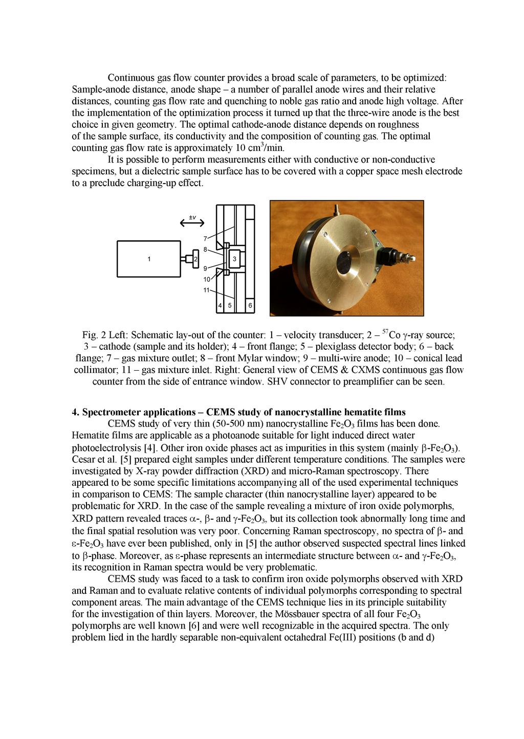
269
270
271 EFFECT OF PREPARATION CONDITIONS ON PARTICLE SIZE DISTRIBUTION IN SILVER NANOPARTICLE HYDROSOLS Sládková M. 1, Vlčková B. 1 Šmejkal P. 1, Šlouf M. 2, Hromádková J. 2 1 Department of Physical and Macromolecular Chemistry, CU in Prague, Czech Republic, MagdiSla@seznam.cz 2 Institute of Macromolecular Chemistry, AS CR, Prague, Czech Republic VLIV PODMÍNEK PŘÍPRAVY NA DISTRIBUCI VELIKOSTÍ NANOČÁSTIC V HYDROSOLECH STŘÍBRNÝCH NANOČÁSTIC Sládková M. 1, Vlčková B. 1 Šmejkal P. 1, Šlouf M. 2, Hromádková J. 2 1 Katedra Fyzikální a Makromolekulární Chemie, UK v Praze, Česká republika, MagdiSla@seznam.cz 2 Institute of Macromolecular Chemistry, AV ČR, Praha, Česká republika Abstract A possibility to affect the process of Ag nanoparticle growth and, consequently, the resulting mean particle sizes and particle size distributions by the rate of addition of the AgNO 3 solution to the NaBH 4 solution during the preparation of Ag nanoparticle hydrosols has been explored. A STEPDOS microprocessor controlled diaphragm metering pump was used to control the rate of the reagent addition, and its values of 200, 300, 400, 500 and 600 µl/min were adopted to prepare different Ag hydrosol samples. The lowest polydispersity of the Ag nanoparticle hydrosol has been achieved at the slowest rate of the AgNO 3 solution addition, i.e. at 200 µl/min, while the largest polydispersity has been encountered in the Ag nanoparticle hydrosol prepared at the addition rate of 600 µl/min. The possibility to control polydispersity of Ag nanoparticle hydrosols by the rate of the reagent addition has thus been demonstrated and found important for their preparations targeted on a desired type of application. Keywords: Ag nanoparticles, Ag hydrosol. Abstrakt V této studii byl zkoumáno, zda proces růstu Ag nanočástic, následně i jejich průměrná velikost a distribuce velikostí, může být ovlivněn rychlostí přídavku roztoku AgNO 3 do roztoku NaBH 4. Za tímto účelem byla použita mikroprocesorem řízená membránová měřící pumpa STEPDOS. Pomocí tohoto přístroje byly připraveny vzorky Ag hydrosolů kontrolovanou rychlostí přídavku roztoku AgNO 3 do roztoku NaBH 4 za konstantní rychlosti míchání 200, 300, 400, 500 a 600 µl/min. Nejmenší polydispersita nanočástic v Ag hydrosolu byla dosažena při nejpomalejší použité rychlosti přídavku roztoku AgNO 3, tj. při rychlosti 200 µl/min, zatím co nejvyšší polydispersita nanočástic v Ag hydrosolu byla zjištěna při použité rychlosti přídavku roztoku AgNO µl/min. Možnost řídit polydispersitu Ag nanočástic pomocí rychlosti přídavku reagentu byla shledána významnou pro cílenou přípravu Ag nanočástic s vlastnostmi dle požadovaného typu aplikace. Introduction Ag nanoparticles and their assemblies are the subject of permanent interest stimulated by their applications as e.g. sensors or light amplifiers [1, 2]. Since the optical responses of these nanoparticles are size-dependent, a common goal of various preparation procedures is to achieve
272 at least a partial control over the mean size and size-distibution of the resulting Ag nanoparticles. The goal of our study has been to explore, whether the process of Ag nanoparticle growth and, consequently, the resulting mean particle sizes and particle size distributions, can be affected by the rate of addition of the AgNO 3 solution to the NaBH 4 solution at constant rpm of the stirrer. Experimental 1. Materials and procedures Materials. Sodium chloride (p.a. Lachema), Silver nitride (p.a. Aldrich) and deionized water. Preparation of Ag hydrosol. Ag hydrosol was prepared by reduction of AgNO 3 by NaBH 4 in aqueous ambient, in particular on a modification [3] of the procedure originally reported in [4]. Briefly, 9 ml of 2.2 x 10⁻³ M aqueous solution of AgNO 3 were added dropwise to rapidly stirred 75 ml of 1.1 x10⁻³ M aqueous solution of NaBH 4 at 2 C. The STEPDOS microprocessor controlled diaphragm metering pump was used to control the rate, and its values of 200, 300, 400, 500 and 600 µl/min were applied to prepare different Ag hydrosol samples. Preparation of samples for TEM measurements. Copper grids for TEM microscopy (Agar Scientific, Ltd.) were pre-treated of a thin carbon layer on their reverse sides. Ag hydrosols were fall a drop onto copper grid. 2. Instrumentation Electronic absorption spectra of Ag hydrosol were measured with a Perkin Elmer Lambda 12 UV-Vis spectrometer. EA spectra are compared in Fig. 1A, 2A, 3A, 4A and 5A. TEM images of the samples were obtained with TECNAI G2.SPIRIT transmission electron microscope. Tem images of Ag nanoparticles are compared in Fig. 1C, 2C, 3C, 4C and 5C. Fig.1 Rate dropwise 200 µl/min A)UV-Vis spectrum of Ag hydrosol, B)Particle size distribution of Ag nanoparticles, C)TEM image of Ag nanoparticles
UV-Vis spectrum of Ag hydrosol, B)Particle size distribution of Ag nanoparticles, C)TEM image of Ag nanoparticles Fig.")
273 Fig.2 Rate dropwise 300 µl/min A)UV-Vis spectrum of Ag hydrosol, B)Particle size distribution of Ag nanoparticles, C)TEM image of Ag nanoparticles Fig.3 Rate dropwise 400 µl/min A)UV-Vis spectrum of Ag hydrosol, B)Particle size distribution of Ag nanoparticles, C)TEM image of Ag nanoparticles Fig.4 Rate dropwise 500 µl/min A)UV-Vis spectrum of Ag hydrosol, B)Particle size distribution of Ag nanoparticles, C)TEM image of Ag nanoparticles
VÝVOJ ULTRAJEMNÍ STRUKTURY V OCELÍCH V PODMÍNKÁCH EXTRÉMNÍ DEFORMACE ECAP
 VÝVOJ ULTRAJEMNÍ STRUKTURY V OCELÍCH V PODMÍNKÁCH EXTRÉMNÍ DEFORMACE ECAP DEVELOPMENT OF ULTRAFINE STRUCTURE IN STEELS IN CONDITIONS OF SEVERE PLASTIC DEFORMATION ECAP Libor KRAUS a, Jozef ZRNÍK a,b, Sergey
Objemové ultrajemnozrnné materiály. Miloš Janeček Katedra fyziky materiálů, MFF UK
 Objemové ultrajemnozrnné materiály Miloš Janeček Katedra fyziky materiálů, MFF UK Definice Objemové ultrajemnozrnné materiály (bulk UFG ultrafine grained materials) Malá velikost zrn (> 1µm resp. 100 nm)
VLIV MIKROSTRUKTURNÍCH ZMĚN NA MECHANICKÉ CHOVÁNÍ HLINÍKU PO EXTRÉMNÍ PLASTICKÉ DEFORMACI (ECAP)
") VLIV MIKROSTRUKTURNÍCH ZMĚN NA MECHANICKÉ CHOVÁNÍ HLINÍKU PO EXTRÉMNÍ PLASTICKÉ DEFORMACI (ECAP) EFFECT OF MICROSTRUCTURE CHANGES ON THE MECHANICAL BEHAVIOUR OF ALUMINUM AFTER SEVERE PLASTIC DEFORMATION
VLIV MIKROSTRUKTURNÍCH ZMĚN NA MECHANICKÉ CHOVÁNÍ HLINÍKU PO EXTRÉMNÍ PLASTICKÉ DEFORMACI (ECAP) EFFECT OF MICROSTRUCTURE CHANGES ON THE MECHANICAL BEHAVIOUR OF ALUMINUM AFTER SEVERE PLASTIC DEFORMATION
VLIV OBSAHU NIKLU NA VLASTNOSTI LKG PO FERITIZAČNÍM ŽÍHÁNÍ EFFECT OF THE CONTENT OF NICKEL ON DI PROPERTIES AFTER FERRITIZATION ANNEALING
 VLIV OBSAHU NIKLU NA VLASTNOSTI LKG PO FERITIZAČNÍM ŽÍHÁNÍ EFFECT OF THE CONTENT OF NICKEL ON DI PROPERTIES AFTER FERRITIZATION ANNEALING Hana Tesařová Bohumil Pacal Ondřej Man VUT-FSI-ÚMVI-OKM, Technická
Sborník vědeckých prací Vysoké školy báňské - Technické univerzity Ostrava číslo 1, rok 2006, ročník LII, řada strojní článek č.
 Sborník vědeckých prací Vysoké školy báňské - Technické univerzity Ostrava číslo 1, rok 2006, ročník LII, řada strojní článek č. 1521 Petr TOMČÍK *, Radim TROJAN **, Petr MOHYLA THE PULSED MAGNETIC TREATMENT
CHAPTER 5 MODIFIED MINKOWSKI FRACTAL ANTENNA
 CHAPTER 5 MODIFIED MINKOWSKI FRACTAL ANTENNA &KDSWHUSUHVHQWVWKHGHVLJQDQGIDEULFDW LRQRIPRGLILHG0LQNRZVNLIUDFWDODQWHQQD IRUZLUHOHVVFRPPXQLFDWLRQ7KHVLPXODWHG DQGPHDVXUHGUHVXOWVRIWKLVDQWHQQDDUH DOVRSUHVHQWHG
VLASTNOSTI OCELI CSN 12050 (DIN C 45) S VELMI JEMNOU MIKROSTRUKTUROU PROPERTIES OF THE C45 DIN GRADE STEEL (CSN 12050) WITH VERY FINE MICROSTRUCTURE
 S VELMI JEMNOU MIKROSTRUKTUROU PROPERTIES OF THE C45 DIN GRADE STEEL (CSN 12050) WITH VERY FINE MICROSTRUCTURE") VLASTNOSTI OCELI CSN 12050 (DIN C 45) S VELMI JEMNOU MIKROSTRUKTUROU PROPERTIES OF THE C45 DIN GRADE STEEL (CSN 12050) WITH VERY FINE MICROSTRUCTURE J. Drnek Z. Nový P. Fišer COMTES FHT s.r.o., Borská
VLASTNOSTI OCELI CSN 12050 (DIN C 45) S VELMI JEMNOU MIKROSTRUKTUROU PROPERTIES OF THE C45 DIN GRADE STEEL (CSN 12050) WITH VERY FINE MICROSTRUCTURE J. Drnek Z. Nový P. Fišer COMTES FHT s.r.o., Borská
The Over-Head Cam (OHC) Valve Train Computer Model
 Valve Train Computer Model") The Over-Head Cam (OHC) Valve Train Computer Model Radek Tichanek, David Fremut Robert Cihak Josef Bozek Research Center of Engine and Content Introduction Work Objectives Model Description Cam Design
The Over-Head Cam (OHC) Valve Train Computer Model Radek Tichanek, David Fremut Robert Cihak Josef Bozek Research Center of Engine and Content Introduction Work Objectives Model Description Cam Design
Výukový materiál zpracovaný v rámci operačního programu Vzdělávání pro konkurenceschopnost
 Výukový materiál zpracovaný v rámci operačního programu Vzdělávání pro konkurenceschopnost Registrační číslo: CZ.1.07/1. 5.00/34.0084 Šablona: II/2 Inovace a zkvalitnění výuky cizích jazyků na středních
HODNOCENÍ VLASTNOSTÍ VÝKOVKŮ ROTORŮ Z OCELI 26NiCrMoV115
 HODNOCENÍ VLASTNOSTÍ VÝKOVKŮ ROTORŮ Z OCELI 26NiCrMoV115 Martin BALCAR a), Václav TURECKÝ a), Libor Sochor a), Pavel FILA a), Ludvík MARTÍNEK a), Jiří BAŽAN b), Stanislav NĚMEČEK c), Dušan KEŠNER c) a)
VLIV GEOMETRIE NÁSTROJE ECAP NA DOSAŽENÉ ZJEMNĚNÍ ZRNA INFLUENCE OF ECAP DIE GEOMETRY ON ACHIEVED UFG
 VLIV GEOMETRIE NÁSTROJE ECAP NA DOSAŽENÉ ZJEMNĚNÍ ZRNA INFLUENCE OF ECAP DIE GEOMETRY ON ACHIEVED UFG Stanislav Rusz a Jan Dutkiewicz b Lubomír Čížek a Jiří Hluchník a a VŠB Technická univerzita Ostrava,
CREEPOVÉ CHOVÁNÍ HLINÍKOVÉ SLITINY Al-3Mg-0,2Sc PŘIPRAVENÉ METODOU ECAP. CREEP BEHAVIOUR OF Al-3Mg-0,2Sc ALLOY PROCESSED BY ECAP METHOD
 CREEPOVÉ CHOVÁNÍ HLINÍKOVÉ SLITINY PŘIPRAVENÉ METODOU ECAP CREEP BEHAVIOUR OF ALLOY PROCESSED BY ECAP METHOD Jiří Dvořák a, Petr Král a, Václav Sklenička a a Ústav fyziky materiálů, Akademie věd České
Gabriela DOROCIAKOVÁ a, Miroslav GREGER a, Radim KOCICH a a Barbora KUŘETOVÁ a
 ZMĚNA STRUKTURY A VLASTNOSTÍ MĚDI PO PROTLAČOVÁNÍ TECHNOLOGIÍ ECAP THE CHANGE OF STRUCTURE AND PROPERTIES OF COPPER AFTER PRESSING BY THE ECAP TECHNOLOGY Gabriela DOROCIAKOVÁ a, Miroslav GREGER a, Radim
MOŽNOSTI VYUŽITÍ MIKROLEGOVANÝCH OCELÍ. Tomáš Schellong Kamil Pětroš Václav Foldyna. JINPO PLUS a.s., Křišťanova 2, 702 00 Ostrava, ČR
 MOŽNOSTI VYUŽITÍ MIKROLEGOVANÝCH OCELÍ Tomáš Schellong Kamil Pětroš Václav Foldyna JINPO PLUS a.s., Křišťanova 2, 702 00 Ostrava, ČR Abstract The proof stress and tensile strength in carbon steel can be
CREEP AUSTENITICKÉ LITINY S KULIČKOVÝM GRAFITEM CREEP OF AUSTENITIC DUCTILE CAST IRON
 METAL 9 9... 9, Hradec nad Moravicí CREEP AUSTENITICKÉ LITINY S KULIČKOVÝM GRAFITEM CREEP OF AUSTENITIC DUCTILE CAST IRON Vlasák, T., Hakl, J., Čech, J., Sochor, J. SVUM a.s., Podnikatelská, 9 Praha 9,
INFLUENCE OF HEAT RE-TREATMENT ON MECHANICAL AND FATIGUE PROPERTIES OF THIN SHEETS FROM AL-ALLOYS. Ivo Černý Dagmar Mikulová
 VLIV TEPELNÉHO PŘEPRACOVÁNÍ NA MECHANICKÉ A ÚNAVOVÉ VLASTNOSTI TENKÝCH PLECHŮ Z AL-SLITIN INFLUENCE OF HEAT RE-TREATMENT ON MECHANICAL AND FATIGUE PROPERTIES OF THIN SHEETS FROM AL-ALLOYS Ivo Černý Dagmar
CREEPOVÉ CHOVÁNÍ ULTRAJEMNOZRNNÉHO HLINÍKU
 CREEPOVÉ CHOVÁNÍ ULTRAJEMNOZRNNÉHO HLINÍKU Jiří Dvořák a, Václav Sklenička a, Milan Svoboda a a Ú fyziky materiálů, Akademie věd České republiky, Žižkova 22, 616 62 Brno, ČR, dvorak@ipm.cz Abstrakt Extrémně
Compression of a Dictionary
 Compression of a Dictionary Jan Lánský, Michal Žemlička zizelevak@matfyz.cz michal.zemlicka@mff.cuni.cz Dept. of Software Engineering Faculty of Mathematics and Physics Charles University Synopsis Introduction
DETERMINATION OF MECHANICAL AND ELASTO-PLASTIC PROPERTIES OF MATERIALS BY NANOINDENTATION METHODS
 DETERMINATION OF MECHANICAL AND ELASTO-PLASTIC PROPERTIES OF MATERIALS BY NANOINDENTATION METHODS HODNOCENÍ MECHANICKÝCH A ELASTO-PLASTICKÝCH VLASTNOSTÍ MATERIÁLŮ VYUŽITÍM NANOINDENTACE Martin Vizina a
SPECIFICATION FOR ALDER LED
 SPECIFICATION FOR ALDER LED MODEL:AS-D75xxyy-C2LZ-H1-E 1 / 13 Absolute Maximum Ratings (Ta = 25 C) Parameter Symbol Absolute maximum Rating Unit Peak Forward Current I FP 500 ma Forward Current(DC) IF
Litosil - application
 Litosil - application The series of Litosil is primarily determined for cut polished floors. The cut polished floors are supplied by some specialized firms which are fitted with the appropriate technical
Melting the ash from biomass
 Ing. Karla Kryštofová Rožnov pod Radhoštěm 2015 Introduction The research was conducted on the ashes of bark mulch, as representatives of biomass. Determining the influence of changes in the chemical composition
INFLUENCE OF TEMPERING ON THE PROPERTIES OF CAST C-Mn STEEL AFTER NORMALIZING AND AFTER INTERCRITICAL ANNEALING. Josef Bárta, Jiří Pluháček
 VLIV POPOUŠTĚNÍ NA VLASTNOSTI LITÉ C-Mn OCELI PO NORMALIZACI A PO INTERKRITICKÉM ŽÍHÁNÍ INFLUENCE OF TEMPERING ON THE PROPERTIES OF CAST C-Mn STEEL AFTER NORMALIZING AND AFTER INTERCRITICAL ANNEALING Josef
Tváření,tepelné zpracování
 tváření, tepelné zpracování Optimalizace řízeného válcování nové konstrukční oceli se zvláštními užitnými vlastnostmi Prof. Ing. Ivo Schindler, CSc., Doc. Dr. Ing. Jaroslav Sojka, VŠB-TU Ostrava, 17. listopadu
Tento materiál byl vytvořen v rámci projektu Operačního programu Vzdělávání pro konkurenceschopnost.
 Tento materiál byl vytvořen v rámci projektu Operačního programu Vzdělávání pro konkurenceschopnost. Projekt MŠMT ČR Číslo projektu Název projektu školy Klíčová aktivita III/2 EU PENÍZE ŠKOLÁM CZ.1.07/1.4.00/21.2146
EXACT DS OFFICE. The best lens for office work
 EXACT DS The best lens for office work EXACT DS When Your Glasses Are Not Enough Lenses with only a reading area provide clear vision of objects located close up, while progressive lenses only provide
Effect of temperature. transport properties J. FOŘT, Z. PAVLÍK, J. ŽUMÁR,, M. PAVLÍKOVA & R. ČERNÝ Č CTU PRAGUE, CZECH REPUBLIC
 Effect of temperature on water vapour transport properties J. FOŘT, Z. PAVLÍK, J. ŽUMÁR,, M. PAVLÍKOVA & R. ČERNÝ Č CTU PRAGUE, CZECH REPUBLIC Outline Introduction motivation, water vapour transport Experimental
Zubní pasty v pozměněném složení a novém designu
 Energy news4 Energy News 04/2010 Inovace 1 Zubní pasty v pozměněném složení a novém designu Od října tohoto roku se začnete setkávat s našimi zubními pastami v pozměněném složení a ve zcela novém designu.
Gymnázium, Brno, Slovanské nám. 7 WORKBOOK. Mathematics. Teacher: Student:
 WORKBOOK Subject: Teacher: Student: Mathematics.... School year:../ Conic section The conic sections are the nondegenerate curves generated by the intersections of a plane with one or two nappes of a cone.
STRUKTURA A VLASTNOSTI OCELI P2-04BCh PO DEFORMACI METODOU ECAP. STRUCTURE AND PROPERTIES OF A P2-04BCh STEEL AFTER ECAP DEFORMATION
 STRUKTURA A VLASTNOSTI OCELI P2-04BCh PO DEFORMACI METODOU ECAP STRUCTURE AND PROPERTIES OF A P2-04BCh STEEL AFTER ECAP DEFORMATION Vlastimil Vodárek a, Miroslav Greger b, Ladislav Kander a a MATERIÁLOVÝ
CREEP INTERMETALICKÉ SLITINY TiAl PRI VELMI MALÝCH RYCHLOSTECH DEFORMACE. CREEP OF INTERMETALLIC ALLOY TiAl AT VERY LOW STRAIN RATES
 CREEP INTERMETALICKÉ SLITINY TiAl PRI VELMI MALÝCH RYCHLOSTECH DEFORMACE CREEP OF INTERMETALLIC ALLOY TiAl AT VERY LOW STRAIN RATES Petr Marecek a Luboš Kloc b Jaroslav Fiala a a Faculty of Chemistry,
VŠB Technical University of Ostrava, Faculty of Mechanical engineering, 17. Listopadu 15, Ostrava Poruba, Czech Republic
 SIMULACE PROTLAČOVÁNÍ SLITIN Al NÁSTROJEM ECAP S UPRAVENOU GEOMETRIÍ A POROVNÁNÍ S EXPERIMENTY Abstrakt Jan Kedroň, Stanislav Rusz, Stanislav Tylšar VŠB Technical University of Ostrava, Faculty of Mechanical
HODNOCENÍ MIKROSTRUKTURY A VLASTNOSTÍ ODLITKŮ ZE SLITINY AZ91HP EVALUATION OF MICROSTRUCTURE AND PROPERTIES OF SAND CAST AZ91HP MAGNESIUM ALLOY
 HODNOCENÍ MIKROSTRUKTURY A VLASTNOSTÍ ODLITKŮ ZE SLITINY AZ91HP EVALUATION OF MICROSTRUCTURE AND PROPERTIES OF SAND CAST AZ91HP MAGNESIUM ALLOY Vít Janík a,b, Eva Kalabisová b, Petr Zuna a, Jakub Horník
ACOUSTIC EMISSION SIGNAL USED FOR EVALUATION OF FAILURES FROM SCRATCH INDENTATION
 AKUSTICKÁ EMISE VYUŽÍVANÁ PŘI HODNOCENÍ PORUŠENÍ Z VRYPOVÉ INDENTACE ACOUSTIC EMISSION SIGNAL USED FOR EVALUATION OF FAILURES FROM SCRATCH INDENTATION Petr Jiřík, Ivo Štěpánek Západočeská univerzita v
Střední průmyslová škola strojnická Olomouc, tř.17. listopadu 49
 Střední průmyslová škola strojnická Olomouc, tř.17. listopadu 49 Výukový materiál zpracovaný v rámci projektu Výuka moderně Registrační číslo projektu: CZ.1.07/1.5.00/34.0205 Šablona: III/2 Anglický jazyk
STŘEDNÍ PŘIROZENÉ DEFORMAČNÍ ODPORY PŘI TVÁŘENÍ OCELÍ ZA TEPLA - VLIV CHEMICKÉHO A STRUKTURNÍHO STAVU
 STŘEDNÍ PŘIROZENÉ DEFORMAČNÍ ODPORY PŘI TVÁŘENÍ OCELÍ ZA TEPLA - VLIV CHEMICKÉHO A STRUKTURNÍHO STAVU MEAN EQUIVALENT STRESS VALUES DURING HOT FORMING OF STEELS - INFLUENCE OF CHEMICAL AND STRUCTURE STATE
MOŽNOSTI TVÁŘENÍ MONOKRYSTALŮ VYSOKOTAVITELNÝCH KOVŮ V OCHRANNÉM OBALU FORMING OF SINGLE CRYSTALS REFRACTORY METALS IN THE PROTECTIVE COVER
 MOŽNOSTI TVÁŘENÍ MONOKRYSTALŮ VYSOKOTAVITELNÝCH KOVŮ V OCHRANNÉM OBALU FORMING OF SINGLE CRYSTALS REFRACTORY METALS IN THE PROTECTIVE COVER Kamil Krybus a Jaromír Drápala b a OSRAM Bruntál, spol. s r.
SEMI-PRODUCTS. 2. The basic classification of semi-products is: standardized semi-products non-standardized semi-products
 Second School Year SEMI-PRODUCTS 1. Semi-products are materials used for further processing. We produce them from incoming materials, for example from ingots, powders and other materials. We most often
CARBONACEOUS PARTICLES IN THE AIR MORAVIAN-SILESIAN REGION
 UHLÍKATÉ ČÁSTICE V OVZDUŠÍ MORAVSKO- SLEZSKÉHO KRAJE CARBONACEOUS PARTICLES IN THE AIR MORAVIAN-SILESIAN REGION Ing. MAREK KUCBEL Ing. Barbora SÝKOROVÁ, prof. Ing. Helena RACLAVSKÁ, CSc. Aim of this work
SVAŘOVÁNÍ KOVOVÝCH MATERIÁLŮ LASEREM LASER WELDING OF METAL MATERIALS
 SVAŘOVÁNÍ KOVOVÝCH MATERIÁLŮ LASEREM LASER WELDING OF METAL MATERIALS Petr AMBROŽ a, Jiří DUNOVSKÝ b a ČVUT v Praze, Fakulta strojní, Výzkumné centrum pro strojírenskou výrobní techniku a technologii,
POSSIBLE GENERALISATION OF DECREASE IN MECHANICAL PROPERTIES OF CARBON STEEL (ČSN ) ON OTHER STEELS
 ON OTHER STEELS") MOŽNOST ZOBECNĚNÍ POKLESU MECHANICKÝCH VLASTNOSTÍ OCELI 12 022 NA DALŠÍ MATERIÁLY POSSIBLE GENERALISATION OF DECREASE IN MECHANICAL PROPERTIES OF CARBON STEEL (ČSN 12 022) ON OTHER STEELS Josef ČMAKAL,
MOŽNOST ZOBECNĚNÍ POKLESU MECHANICKÝCH VLASTNOSTÍ OCELI 12 022 NA DALŠÍ MATERIÁLY POSSIBLE GENERALISATION OF DECREASE IN MECHANICAL PROPERTIES OF CARBON STEEL (ČSN 12 022) ON OTHER STEELS Josef ČMAKAL,
STLAČITELNOST. σ σ. během zatížení
 STLAČITELNOST Princip: Naneseme-li zatížení na zeminu, dojde k porušení rovnováhy a dochází ke stlačování zeminy (přemístňují se částice). Stlačení je ukončeno jakmile nastane rovnováha mezi působícím
VLIV TEPELNÉHO ZPRACOVÁNÍ NA STRUKTURU SLITINY HLINÍKU AA7075 PO INTENZIVNÍ PLASTICKÉ DEFORMACI METODOU ECAP
 VLIV TEPELNÉHO ZPRACOVÁNÍ NA STRUKTURU SLITINY HLINÍKU AA707 PO INTENZIVNÍ PLASTICKÉ DEFORMACI METODOU ECAP EFFECT OF HEAT TREATMENT ON THE STRUCTURE OF THE ALUMINIUM ALLOY AA707 SUBJECTED TO INTENSIVE
Czech Republic. EDUCAnet. Střední odborná škola Pardubice, s.r.o.
 Czech Republic EDUCAnet Střední odborná škola Pardubice, s.r.o. ACCESS TO MODERN TECHNOLOGIES Do modern technologies influence our behavior? Of course in positive and negative way as well Modern technologies
STUDY OF PLASTIC DEFORMATION OF MAGNESIUM ALLOYS WITH GRADUATE ALUMINIUM CONTENT
 Acta Metallurgica Slovaca, 12, 2006, 4 (490-496) 490 STUDY OF PLASTIC DEFORMATION OF MAGNESIUM ALLOYS WITH GRADUATE ALUMINIUM CONTENT Čížek L. 1, Kocich R. 1, Greger M. 1, Praźmowski M. 2, Tański T. 3
Standardní řada lisů Standard range of presses: 1000 600 340 14-85 280 2000 x 1200 900. 260 2000 x 1200 900. 630 500 89 10 80 500 x 500 560
 ZS ZS ydraulické čtyřsloupové lisy ZS jsou produkční lisy určené pro tažení, stříhání a jiné tvářecí práce. Standardní a zvláštní příslušenství je obdobné jako u lisů typu Z. Rám a rozměry lisu jsou přizpůsobovány
VYSOKÁ ŠKOLA HOTELOVÁ V PRAZE 8, SPOL. S R. O.
 VYSOKÁ ŠKOLA HOTELOVÁ V PRAZE 8, SPOL. S R. O. Návrh konceptu konkurenceschopného hotelu v době ekonomické krize Diplomová práce 2013 Návrh konceptu konkurenceschopného hotelu v době ekonomické krize Diplomová
VLIV TEPELNÉHO ZPRACOVÁNÍ NA VLASTNOSTI JEMNOZRNNÝCH SVAŘITELNÝCH OCELÍ PRO TENKOSTĚNNÉ ODLITKY
 VLIV TEPELNÉHO ZPRACOVÁNÍ NA VLASTNOSTI JEMNOZRNNÝCH SVAŘITELNÝCH OCELÍ PRO TENKOSTĚNNÉ ODLITKY INFLUENCE OF HEAT TREATMENT ON PROPERTIES OF FINE-GRAINED WELDABLE STEELS FOR THIN-WALLED CASTINGS Jiří Cejp
Transportation Problem
 Transportation Problem ١ C H A P T E R 7 Transportation Problem The transportation problem seeks to minimize the total shipping costs of transporting goods from m origins (each with a supply s i ) to n
DATA SHEET. BC516 PNP Darlington transistor. technický list DISCRETE SEMICONDUCTORS Apr 23. Product specification Supersedes data of 1997 Apr 16
 zákaznická linka: 840 50 60 70 DISCRETE SEMICONDUCTORS DATA SHEET book, halfpage M3D186 Supersedes data of 1997 Apr 16 1999 Apr 23 str 1 Dodavatel: GM electronic, spol. s r.o., Křižíkova 77, 186 00 Praha
STRUKTURNÍ A FÁZOVÁ ANALÝZA OCELI T23 STRUCTURE AND PHASE ANALYSIS OF T23 STEEL
 STRUKTURNÍ A FÁZOVÁ ANALÝZA OCELI T23 STRUCTURE AND PHASE ANALYSIS OF T23 STEEL Marie Svobodová a,b Jindřich Douda b František Hnilica b Josef Čmakal b Jiří Dubský c a KMAT FJFI ČVUT, Trojanova 13, 120
PLASTICKÉ VLASTNOSTI VYSOKOPEVNOSTNÍCH MATERIÁLŮ DĚLENÝCH NESTANDARDNÍMI TECHNOLOGIEMI
 PLASTICKÉ VLASTNOSTI VYSOKOPEVNOSTNÍCH MATERIÁLŮ DĚLENÝCH NESTANDARDNÍMI TECHNOLOGIEMI PLASTIC PROPERTIES OF HIGH STRENGHT STEELS CUTTING BY SPECIAL TECHNOLOGIES Pavel Doubek a Pavel Solfronk a Michaela
OPTIMALIZACE REŽIMU TEPELNÉHO ZPRACOVÁNÍ PRO ZVÝŠENÍ MECHANICKÝCH VLASTNOSTÍ SLITINY ALSI9Cu2Mg
 OPTIMALIZACE REŽIMU TEPELNÉHO ZPRACOVÁNÍ PRO ZVÝŠENÍ MECHANICKÝCH VLASTNOSTÍ SLITINY ALSI9Cu2Mg OPTIMIZATION OF HEAT TREATMENT CONDITIONS TO IMPROVE OF MECHANICAL PROPETIES OF AlSi9Cu2Mg ALLOY Jan Šerák,
Vliv metody vyšetřování tvaru brusného kotouče na výslednou přesnost obrobku
 Vliv metody vyšetřování tvaru brusného kotouče na výslednou přesnost obrobku Aneta Milsimerová Fakulta strojní, Západočeská univerzita Plzeň, 306 14 Plzeň. Česká republika. E-mail: anetam@kto.zcu.cz Hlavním
MODELOVÁNÍ A MĚŘENÍ DEFORMACE V TAHOKOVU
 . 5. 9. 007, Podbanské MODELOVÁNÍ A MĚŘENÍ DEFORMACE V TAHOKOVU Zbyšek Nový, Michal Duchek, Ján Džugan, Václav Mentl, Josef Voldřich, Bohuslav Tikal, Bohuslav Mašek 4 COMTES FHT s.r.o., Lobezská E98, 00
Recenze: Ing. Radovan Bureš, CSc.
 Hutnické listy č./00, roč. LXIII Methods of Preparation of Based Alloys Metody přípravy slitin na bázi Ing. Petr Štěpán, Doc. Dr. Ing. Monika Losertová, Ing. Daniel Petlák, Prof. Ing. Drápala Jaromír,
STUDIUM ODUHLIČENÍ POVRCHOVÝCH VRSTEV LOŽISKOVÝCH OCELÍ 100Cr6. RESEARCH OF DECARBURIZATION SURFACE LAYER OF BEARING STEEL 100Cr6
 STUDIUM ODUHLIČENÍ POVRCHOVÝCH VRSTEV LOŽISKOVÝCH OCELÍ 00Cr6 RESEARCH OF DECARBURIZATION SURFACE LAYER OF BEARING STEEL 00Cr6 Petr Dostál a Jana Dobrovská b Jaroslav Sojka b Hana Francová b a Profi am
POVRCHOVÉ VYTVRZENÍ PM NÁSTROJOVÉ OCELI LEGOVANÉ NIOBEM PLAZMOVOU NITRIDACÍ SURFACE HARDENING OF NIOBIUM-CONTAINING PM TOOL STEEL BY PLASMA NITRIDING
 POVRCHOVÉ VYTVRZENÍ PM NÁSTROJOVÉ OCELI LEGOVANÉ NIOBEM PLAZMOVOU NITRIDACÍ SURFACE HARDENING OF NIOBIUM-CONTAINING PM TOOL STEEL BY PLASMA NITRIDING P. Novák, D. Vojtech, J. Šerák Ústav kovových materiálu
STUDIUM ELEKTROCHEMICKÝCH KOROZNÍCH JEVŮ DVOUFÁZOVÝCH OCELÍ ZA POUŽITÍ METODY SRET.
 STUDIUM ELEKTROCHEMICKÝCH KOROZNÍCH JEVŮ DVOUFÁZOVÝCH OCELÍ ZA POUŽITÍ METODY SRET. STUDY OF ELECTROCHEMICAL CORROSION PHENOMENA OF DUPLEX STAINLESS STEELS BY USE OF SRET METHODS Petr Kubečka a Vladimír
X-RAY EXAMINATION OF THE FATIGUE PROCESS RENTGENOGRAFICKÉ ZKOUMÁNÍ ÚNAVOVÉHO PROCESU
 X-RAY EXAMINATION OF THE FATIGUE PROCESS RENTGENOGRAFICKÉ ZKOUMÁNÍ ÚNAVOVÉHO PROCESU J.Fiala *, P.Mazal **, M.Kolega *, P.Liškutín ** * University of West Bohemia Plzeň CZ ** Brno University of Technology
VLIV VODÍKU NA MECHANICKÉ VLASTNOSTI SUPERSLITINY IN738LC HYDROGEN EFFECT ON MECHANICAL PROPERTIES OF IN738LC SUPERALLOY
 VLIV VODÍKU NA MECHANICKÉ VLASTNOSTI SUPERSLITINY IN738LC HYDROGEN EFFECT ON MECHANICAL PROPERTIES OF IN738LC SUPERALLOY Monika LOSERTOVÁ, Kateřina KONEČNÁ, Jan JUŘICA, Petr JONŠTA VŠB-TU Ostrava, 17.
FIRE INVESTIGATION. Střední průmyslová škola Hranice. Mgr. Radka Vorlová. 19_Fire investigation CZ.1.07/1.5.00/
 FIRE INVESTIGATION Střední průmyslová škola Hranice Mgr. Radka Vorlová 19_Fire investigation CZ.1.07/1.5.00/34.0608 Výukový materiál Číslo projektu: CZ.1.07/1.5.00/21.34.0608 Šablona: III/2 Inovace a zkvalitnění
PC/104, PC/104-Plus. 196 ept GmbH I Tel. +49 (0) / I Fax +49 (0) / I I
 / I Fax +49 (0) / I I") E L E C T R O N I C C O N N E C T O R S 196 ept GmbH I Tel. +49 (0) 88 61 / 25 01 0 I Fax +49 (0) 88 61 / 55 07 I E-Mail sales@ept.de I www.ept.de Contents Introduction 198 Overview 199 The Standard 200
E L E C T R O N I C C O N N E C T O R S 196 ept GmbH I Tel. +49 (0) 88 61 / 25 01 0 I Fax +49 (0) 88 61 / 55 07 I E-Mail sales@ept.de I www.ept.de Contents Introduction 198 Overview 199 The Standard 200
THE ROLE OF A COOLING RATE IN THERMO-MECHANICAL TREATMENT WITH INCORPORATED Q-P PROCESS
 VÝZNAM RYCHLOSTI OCHLAZOVÁNÍ V TEPELNĚ-MECHANICKÉM ZPRACOVÁNÍ ZAHRNUJÍCÍM Q-P PROCES THE ROLE O A COOLING RATE IN THERMO-MECHANICAL TREATMENT WITH INCORPORATED Q-P PROCESS Bohuslav MAŠEK, Ludmila KUČEROVÁ,
23. dny tepelného zpracování 23 rd International Conference on Heat Treatment
 Asociace pro tepelné zpracování kovů Association for Heat Treatment of Metals ECOSOND s.r.o. Česká společnosti pro nové materiály a technologie Czech Society for New Materials and Technologies Ústav fyziky
Petr Bednář managing director
 PRESENTATION Petr Bednář managing director Company profile Designing office Petr Bednář Tebeco was established in 2004. At the beginning the company was mainly focusing on mechanical-engineering consulting
Objemové ultrajemnozrnné materiály a jejich příprava. Doc. RNDr. Miloš Janeček CSc. Katedra fyziky materiálů
 Objemové ultrajemnozrnné materiály a jejich příprava Doc. RNDr. Miloš Janeček CSc. Katedra fyziky materiálů Definice Definice objemových ultrajemnozrnných (bulk UFG ultrafine grained) materiálů: Malá velikost
Introduction to MS Dynamics NAV
 Introduction to MS Dynamics NAV (Item Charges) Ing.J.Skorkovský,CSc. MASARYK UNIVERSITY BRNO, Czech Republic Faculty of economics and business administration Department of corporate economy Item Charges
1173 K K 1373 K 0 0,2 0,4 0,6 0,8. 5 1/s 10 1/s 50 1/s /s. p C. p C. p5 900 C ,1 0,2 0,3 0,4 0,5 0,6 0,7 0,8
 Hutnické listy č.3/29 Tváření, tepelné zpracování tváření, tepelné zpracování Stress-strain Behaviour and Softening in Manganese TWIP Steel Tested in Thermal-mechanical Simulator Plastometrické výsledky
CZ.1.07/2.3.00/
 Přehled vědecko-výzkumné, výukové a další činnosti Outline of research, educational and other activities Petr Šperka Mentor: prof. Ing. Martin Hartl, Ph.D. Institute of Machine and Industrial Design Faculty
MODELS OF MEAN FLOW STRESS AND STRUCTURE EVOLUTION OF IRON ALUMINIDES IN HOT FORMING
 Acta Metallurgica Slovaca, 13, 2007, 4 (618-624 618 MODELS OF MEAN FLOW STRESS AND STRUCTURE EVOLUTION OF IRON ALUMINIDES IN HOT FORMING Suchánek P. 1, Schindler I. 1, Kulveitová H. 1, Kratochvíl P. 2,
Biosensors and Medical Devices Development at VSB Technical University of Ostrava
 VŠB TECHNICAL UNIVERSITY OF OSTRAVA FACULTY OF ELECTRICAL ENGINEERING AND COMPUTER SCIENCE Biosensors and Medical Devices Development at VSB Technical University of Ostrava Ing. Martin Černý Ph.D. and
Klepnutím lze upravit styl předlohy. nadpisů. nadpisů.
 1/ 13 Klepnutím lze upravit styl předlohy Klepnutím lze upravit styl předlohy www.splab.cz Soft biometric traits in de identification process Hair Jiri Prinosil Jiri Mekyska Zdenek Smekal 2/ 13 Klepnutím
Air Quality Improvement Plans 2019 update Analytical part. Ondřej Vlček, Jana Ďoubalová, Zdeňka Chromcová, Hana Škáchová
 Air Quality Improvement Plans 2019 update Analytical part Ondřej Vlček, Jana Ďoubalová, Zdeňka Chromcová, Hana Škáchová vlcek@chmi.cz Task specification by MoE: What were the reasons of limit exceedances
VZTAH MEZI MIKROSTRUKTUROU A VLASTNOSTMI ULTRAJEMNOZRNNÉHO HLINÍKU PRIPRAVENÉHO TECHNIKOU ECAP
 VZTAH MEZI MIKROSTRUKTUROU A VLASTNOSTMI ULTRAJEMNOZRNNÉHO HLINÍKU PRIPRAVENÉHO TECHNIKOU ECAP Petr Král 1), Jirí Dvorák 1), Milan Svoboda 1), Václav Sklenicka 1) 1) Ústav fyziky materiálu,akademie ved
Střední průmyslová škola strojnická Olomouc, tř.17. listopadu 49
 Střední průmyslová škola strojnická Olomouc, tř.17. listopadu 49 Výukový materiál zpracovaný v rámci projektu Výuka moderně Registrační číslo projektu: CZ.1.07/1.5.00/34.0205 Šablona: III/2 Anglický jazyk
VLIV STRUKTURNÍCH VAD NA ÚNAVOVÉ CHOVÁNÍ Mg SLITINY AZ91 LITÉ DO PÍSKU
 VLIV STRUKTURNÍCH VAD NA ÚNAVOVÉ CHOVÁNÍ Mg SLITINY AZ91 LITÉ DO PÍSKU EFFECT OF STRUCTURAL DEFECTS ON THE FATIGUE BEHAVIOUR OF SAND-CAST Mg ALLOY AZ91 Hnilica František a), Ocenášek Vladivoj b) UJP PRAHA
GUIDELINES FOR CONNECTION TO FTP SERVER TO TRANSFER PRINTING DATA
 GUIDELINES FOR CONNECTION TO FTP SERVER TO TRANSFER PRINTING DATA What is an FTP client and how to use it? FTP (File transport protocol) - A protocol used to transfer your printing data files to the MAFRAPRINT
Association for the Heat Treatment of Metals. Program. Chemicko-tepelné zpracování kovových povrchů Chemichal Heat Treatment of Metal Surfaces
 Association for the Heat Treatment of Metals Program Chemicko-tepelné zpracování kovových povrchů Chemichal Heat Treatment of Metal Surfaces 24. - 25.11. 2015 24 25 November 2015 Jihlava, Czech Republic
Why PRIME? 20 years of Erasmus Programme Over 2 million students in total Annually
 What is PRIME? Problems of Recognition In Making Erasmus European-wide research project Conducted by ESN with the support of the European Commission Two editions: 1 st in 2009 Follow-up in 2010 Why PRIME?
Czech Technical University in Prague DOCTORAL THESIS
 Czech Technical University in Prague Faculty of Nuclear Sciences and Physical Engineering DOCTORAL THESIS CERN-THESIS-2015-137 15/10/2015 Search for B! µ + µ Decays with the Full Run I Data of The ATLAS
TKGA3. Pera a klíny. Projekt "Podpora výuky v cizích jazycích na SPŠT"
 Projekt "Podpora výuky v cizích jazycích na SPŠT" Pera a klíny TKGA3 Tento projekt je spolufinancován Evropským sociálním fondem a státním rozpočtem ČR Pera a klíny Pera a klíny slouží k vytvoření rozbíratelného
PAINTING SCHEMES CATALOGUE 2012
 Evektor-Aerotechnik a.s., Letecká č.p. 84, 686 04 Kunovice, Czech Republic Phone: +40 57 57 Fax: +40 57 57 90 E-mail: sales@evektor.cz Web site: www.evektoraircraft.com PAINTING SCHEMES CATALOGUE 0 Painting
Dynamic Development of Vocabulary Richness of Text. Miroslav Kubát & Radek Čech University of Ostrava Czech Republic
 Dynamic Development of Vocabulary Richness of Text Miroslav Kubát & Radek Čech University of Ostrava Czech Republic Aim To analyze a dynamic development of vocabulary richness from a methodological point
Moderní technologie dokončování velmi přesných děr vystržováním a její vliv na užitné vlastnosti výrobků
 Moderní technologie dokončování velmi přesných děr vystržováním a její vliv na užitné vlastnosti výrobků Stanislav Fiala 1, Ing. Karel Kouřil, Ph.D 1, Jan Řehoř 2. 1 HAM-FINAL s.r.o, Vlárská 22, 628 00
ASTM A694 F60 - TEPELNÉ ZPRACOVÁNÍ A MECHANICKÉ VLASTNOSTI ASTM A694 F60 HEAT TREATMENT AND MECHANICAL PROPERTIES
 ASTM A694 F60 - TEPELNÉ ZPRACOVÁNÍ A MECHANICKÉ VLASTNOSTI ASTM A694 F60 HEAT TREATMENT AND MECHANICAL PROPERTIES Martin BALCAR, Jaroslav NOVÁK, Libor SOCHOR, Pavel FILA, Ludvík MARTÍNEK ŽĎAS, a.s., Strojírenská
VÝZKUM VLASTNOSTÍ SMĚSI TEKBLEND Z HLEDISKA JEJÍHO POUŽITÍ PRO STAVBU ŽEBRA
 Vladimír Petroš, VŠB Technická univerzita Ostrava, 17. listopadu 15/2172, 708 33 Ostrava, Poruba, tel.: +420 597325287, vladimir.petros@vsb.cz; Jindřich Šancer, VŠB Technická univerzita Ostrava, 17. listopadu
materiálové inženýrství
 Materiálové inženýrství Hutnické listy č.1/28 materiálové inženýrství Vliv extrémní plastické deformace metodou ECAP na strukturu a vlastnosti oceli P2-4BCh Prof. Ing.Vlastimil Vodárek,CSc. 1, Doc. Ing.
Střední průmyslová škola strojnická Olomouc, tř.17. listopadu 49
 Střední průmyslová škola strojnická Olomouc, tř.17. listopadu 49 Výukový materiál zpracovaný v rámci projektu Výuka moderně Registrační číslo projektu: CZ.1.07/1.5.00/34.0205 Šablona: III/2 Anglický jazyk
Characterization of soil organic carbon and its fraction labile carbon in ecosystems Ľ. Pospíšilová, V. Petrášová, J. Foukalová, E.
 Characterization of soil organic carbon and its fraction labile carbon in ecosystems Ľ. Pospíšilová, V. Petrášová, J. Foukalová, E. Pokorný Mendel University of Agriculture and Forestry, Department of
SPECIAL FORMING METHODS. Use: It is used for the production of cylindrical and conical parts of exact shapes, which needn t be further machined.
 Third School Year 1) Rotary die SPECIAL FORMING METHODS Use: It is used for the production of cylindrical and conical parts of exact shapes, which needn t be further machined. Basics: Hammers with hardened
Stojan pro vrtačku plošných spojů
 Střední škola průmyslová a hotelová Uherské Hradiště Kollárova 617, Uherské Hradiště Stojan pro vrtačku plošných spojů Závěrečný projekt Autor práce: Koutný Radim Lukáš Martin Janoštík Václav Vedoucí projektu:
T E S T R E P O R T No. 18/440/P124
 CENTRUM STAVEBNÍHO INŽENÝRSTVÍ a.s. Zkušebna fyzikálních vlastností materiálů, konstrukcí a budov - Praha Zkušební laboratoř č. 1007.4 akreditovaná ČIA dle ČSN EN ISO/IEC 17025 Pražská 16, 102 00 Praha
By David Cameron VE7LTD
 By David Cameron VE7LTD Introduction to Speaker RF Cavity Filter Types Why Does a Repeater Need a Duplexer Types of Duplexers Hybrid Pass/Reject Duplexer Detail Finding a Duplexer for Ham Use Questions?
Aplikace matematiky. Dana Lauerová A note to the theory of periodic solutions of a parabolic equation
 Aplikace matematiky Dana Lauerová A note to the theory of periodic solutions of a parabolic equation Aplikace matematiky, Vol. 25 (1980), No. 6, 457--460 Persistent URL: http://dml.cz/dmlcz/103885 Terms
Comparison of Two Designs for the Spiral Casing of the Fan Grinding Mill. Porovnání dvou konstrukčních variant spirálové skříně ventilátorového mlýna
 Comparison of Two Designs for the Spiral Casing of the Fan Grinding Mill Porovnání dvou konstrukčních variant spirálové skříně ventilátorového mlýna Richard KLUČKA 1 Abstract: This work deals with comparison
POČET ROČNÍKŮ JEHLIC POPULACÍ BOROVICE LESNÍ. Needle year classes of Scots pine progenies. Jarmila Nárovcová. Abstract
 POČET ROČNÍKŮ JEHLIC POPULACÍ BOROVICE LESNÍ Needle year classes of Scots pine progenies Jarmila Nárovcová Výzkumný ústav lesního hospodářství a myslivosti, v. v. i. Výzkumná stanice Opočno Na Olivě 550
VERIFICATION OF DEFORMATION BEHAVIOUR OF BULK TRIP STEEL
 VERIFICATION OF DEFORMATION BEHAVIOUR OF BULK TRIP STEEL Jozef ZRNIK 1, Ondrej MURANSKY 2, Zbyšek NOVY 1, Peter SLAMA 1 1 COMTES FHT Inc., Prumyslova 995, 33441 Dobrany, Czech Republic, jozef.zrnik@comtesfht.cz
Influence of Pre-Oxidation on Mechanical Properties of Zr1Nb Alloy
 Influence of Pre-Oxidation on Mechanical Properties of Zr1Nb Alloy Olga Bláhová New Technologies - Research Centre in Westbohemian Region University of West Bohemia, Plzen 1 Zirconium Alloys The use of
Klepnutím lze upravit styl předlohy. Klepnutím lze upravit styl předlohy. nadpisů. nadpisů. Aleš Křupka.
 1 / 13 Klepnutím lze upravit styl předlohy Klepnutím lze upravit styl předlohy www.splab.cz Aleš Křupka akrupka@phd.feec.vutbr.cz Department of Telecommunications Faculty of Electrotechnical Engineering